
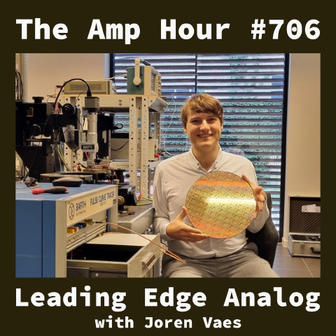
#706 – Leading Edge Analog with Joren Vaes
Download episode · 103 MB
Also on Apple · Spotify · YouTube · RSS
Show Notes
Welcome Joren Vaes, design engineer at SOFICS
- Simulation is critical when designing analog devices based on a PDK from the fab
- Parasitics are significant, especially with new nodes having upwards of 16 metal layers
- Chris complained about a class where the professor made them draw planar structures with graph paper with colored pencils
- Large fabs on leading edge nodes have 1800 page textbook of rules
- Because the constraints get tighter, that book gets longer for each node
- 2 nm mass production on finfet currently with TSMC
- 22 was the last classic cmos
- Finfet, looks like a devil
- 'gate all around' / nanosheet
- CFET (complementary field effect transistor) is next
- Joren really gets Maxwells Equations...as you have to at super high speeds
- SOFICS are making phy's / IP blocks
- Amplifiers that are DC to 50 GHz
- Making a datasheet for the resulting IP block
- Joren got his PhD working on millimeter wave applications
- It's all just physics
- Using coils to impedance match between layers
- Reflecting off of different materials at angles is Snells law (not lorentz equation) and that extends to different materials at different wavelengths
- Cables are very lossy at 100 GHz...dBs per cm
- Parasitics impact every part of the design process
- Wireline community - name for the high speed interfaces, including research in the space
- Most transistor threshhold voltages that Joren works with are ... 750 mV!
- Voltage dependent drc rules
- Electromigration - holes in wires from electrons
- ESD is a big part of the business, and a large source of parasitics
- New product development for IP blocks
- Working with customers and Foundry at the 2 nm node
- Design companies need to be paying 100s of thousands to software providers
- After, it goes to spice and schedmatic
- Joren decides whether to jump in on layout
- LVS - layout vs schematic
- Parasitic extraction (spice netlist)
- PDKs define how you can do the layout stage
- Lower cost tools exist but more expensive tools have tooling that tells you when you're violating DRC
- 3 main vendors
- Cadence
- Synopsis
- Siemens (Calibre)
- Foundries soemtimes only support one tool
- Doing test wafers allows testing of structures. They often get MPW at a discount from the fab (since they're often testing new processes as well)
- How do they test with packaging options?
- 'low speed' can be die bonded or pcb mounted
- high speed does on wafer probing (with veeeery expensive probes)
- Check out Sofics.com for more info on the company. They also have a blog with a great name.
- Follow or connect with Joren on LinkedIn
Transcript
Chris Gammell: This is the Up Hour Podcast. Released October 18th, 2025. Episode 706. Leading Edge Analog with Joren Voss. Welcome to the Amp Hour. I'm Chris Gammell of Contextual Electronics.
Joren Vaes: And I'm Joren, a high-speed designer from Sulphix.
Chris Gammell: Hey, Joren. How are you doing?
Joren Vaes: I'm doing good. How are you, Chris?
Chris Gammell: I'm good. I'm really excited to talk to someone like you because we've been talking about open source silicon in the past, and we've talked about ship design in larger places. Not so much, though, on the analog, low-level, making signals wiggle up and down and actually doing not just zeros and ones, all the stuff in between. It sounds like we're going to be talking about that here today.
Joren Vaes: Yeah, the real world's analog, right?
Chris Gammell: That's right. Yeah. I mean, the thing I don't really get from the silicon side of things is you get these tools from the foundries, but then you have to do all this magical math in between. And it seems really tough. And it seems like there's a lot of simulation and kind of figuring out as you go along and trusting in the tools. And then at the end, yeah, they make what you tell them to. But you have to make sense of all the output that you've put into these shapes on planer. Yeah.
Joren Vaes: Yeah. So, indeed, I think what you mentioned there is kind of the real biggest step that I had to make when I went into IC design is the difference between hardware design, PCB-level design, and IC design is the level of simulation and modeling that we can do in the design stage for analog and for high speed. Digital designers do this in a different way. But for analog, we have these models for each transistor that are extremely complicated, hundreds of parameters inside of the model that's provided by the foundry in the process development kit, as they call it. And so, when we're designing, we can really get a very high degree of confidence in that what we are designing will work the way we intend, because we can do extremely in-depth simulation on the individual transistor level. And in a lot of cases, if you do your job well, we can get within a few percent in the real silicon if you really model everything. Even with the parasitics, we have tools that will extract. So, you do the design on a transistor level in the schematic, right? And then you have to actually, like on a PCB, do the layout, connect everything up. But in silicon, especially in the newer nodes where you have 14, 15, 18 metal layers, you'll have a lot of metal parasitics, a lot of additional capacitance, a lot of additional resistance. And all of this also impacts your circuit performance. But again, we have like very complicated tools that will think about this very hard on very big servers. And they will come up with parasitic models of add a lot of transistors. You go from a schematic that might have had 30, 40 transistor devices to schematics that without exaggerating have 2 million, 3 million devices, just because you have so much parasitics in these very complicated networks. And then you can, again, simulate them and really get a good idea of what we will get when we get the silicon back from the foundry.
Chris Gammell: Okay. So, I did very, very poorly in my analog chip design class in university, which is 20 plus years ago now. But my teacher at the time, who I've talked about on the show, I've been angry with him. He insisted, he insisted that we use colored pencils and graph paper and draw transistor shapes. So, how much of your day-to-day work is drawing boxes with colored pencils? More than I would like to admit, I think. Ah, damn it. That was not the answer I hoped for. Oh, man. Well, it also depends on who you talk to in our field. I thought it was just going to be computer tools all day long. Really?
Joren Vaes: You're using graph paper and colored pencils? Well, not graph paper and colored pencils. So, the layout that we do of the transistors, really, in a lot of cases, we go down to drawing the individual rectangle. Like, this is going to be a P plus implant in the silicon. Sure, sure. This is where we're going to draw oxide and so on by hand.
Chris Gammell: So, this is just to offset it from like a standard cell where a digital designer might be like, this is a NAND gate. You're like, a NAND gate? Get out of here with your NAND gate. I'm going to put in doping levels on a P well or something.
Joren Vaes: Well, we don't necessarily get to pick the doping levels on a very granular level. We get often what they would call different threshold voltage versions of a transistor. So, you might get a very low threshold transistor and then you have a standard and a high, right? And you get to pick that, but that's about it. But we do really have the ability to draw these individual boxes.
Chris Gammell: Well, okay. So, maybe we need to talk a little bit about... So, now I'm drawing from multiple experiences. One, my hateful experience of graph paper, but the other one being working in a fab and understanding a little bit about the process layers and stuff like that. So, like you get a PDK from a foundry and they are giving you these, you know, like a multiple choice kind of selection for a transistor. Is that right? Or is it more of multiple choice for where you're opening up a mask on a certain layer?
Joren Vaes: It's a bit of both, right? So, we... Because we draw the transistor by drawing... Well, historically, you really draw where the openings in the mask would come. Now, there's a lot of post-processing we don't see, but that's another story. But we really do draw like, this is where the poly is going to come and this is where the fusion is going to come and so on. But we get huge rule books. I know when I did some PCB design, you had maybe a few hundred rules, right? But on our latest tape out in one of very high-end processes, we had a textbook that was 1,800 pages of rules, right? And that specifies like to a very granular level, like this you're allowed to do and this you're not. And it's not just like, oh, your minimum trace width is this much nanometers and your minimum spacing is that much nanometers. It goes like, if you draw a 10 nanometer trace, you need to keep a 10 nanometer space to the next trace. And otherwise, you have to draw a 12 nanometer trace and then you have to keep a 14 nanometer space. Or if you draw a 60 nanometer, then it's this much. And when you go above 25 nanometers, you can scale it in any intermediate size, right? And that's the kind of thing you would do. Or maybe you can put one via or you could put three vias. You're not allowed to put two vias. If your three vias are in this specific pattern, that's also not allowed unless there's a fourth via. So it gets incredibly complicated. But that's kind of the way that we then also ensure that, well, the foundry ensures that what we draw and what we can then simulate will actually behave the way it does because there's so much insane physics that goes on in these FinFed nodes and in nanosheet nodes to actually make this work.
Chris Gammell: You know, so you've been in the industry for a little while, but like, does the textbook get longer each successive node?
Joren Vaes: Yes. So yeah, definitely. So back when I did some work during my PhD in 45 nanometer and 28 nanometer silicon, and then the rule books were 400, 500 pages. And then now with each new generation of FinFed or now nanosheet, as TSMC is moving over to the next gen after FinFed, the rule books just keep getting more and more complicated. And you get into these very complicated multi-patterning rules. As I said, like these, you have to follow a specific grid pattern and so on.
Chris Gammell: What is a kind of a leading edge node these days, like for an analog process? Like what would be an expectation? You mentioned FinFed, and that's tied to certain node numbers and stuff.
Joren Vaes: But what are we at right now? Two nanometers at TSMC is, I think, coming out for mass production later this year or early next year. And then we're actually moving away from FinFed. So with FinFed, we, well, I say we, TSMC or Samsung Foundry grew little mountains on which they fold the transistor. And that way you can get more transistor per unit area of the process because you're kind of folding them over. I don't know anything about this. This is cool. Yeah. So, so what they did is you, the problem you had with planar technologies, right? So the 28 and the 22 nanometer node at TSMC were the last classic CMOS technologies where you really have a planar transistor. So you have the wafer and the transistor is flat on top of the wafer. But the problem you actually have is that the drain and the source contact are so close together that they have a lot of impact on the field underneath the gate and the gate itself has limited control over, over the field. Right. And so you have very leaky device, which is undesirable, especially the digital guys don't really like this because a lot of the power that you dissipate is just leakage. It's just transistors that are supposed to be off, but they're not off.
Chris Gammell: I remember that there was a, there was a formula for that, right? It was like the clock speed and the capacitance, which the gate stuff did. And there was a four in there. Yes.
Joren Vaes: Well, I'm not a digital designer, so I don't worry about it.
Chris Gammell: Okay. Yeah. I just remember like someone pointed at that, that whatever that free, whatever that formula is. And they pointed at that because, and like, that was always the reason, maybe we talked about on the show even, that was the reason that we don't have 10 gigahertz devices as well. Right. Because like, it just scales like crazy. Maybe the fourth power instead. I don't know. But it was like something that was definitely one of the reasons why we don't, the gigahertz hasn't, haven't climbed in lockstep like, like they had been.
Joren Vaes: And so what they did then, because they, these transistors were so bad at being turned off is that they actually went to the third dimension. I think Intel was first with this Intel's 22 node. And so they kind of grow a ridge called a fin.
Chris Gammell: Yeah.
Joren Vaes: Right. It looked like devil horns. If you looked at the cross section, right. Wasn't that the fin? Yeah, exactly. And then the transistor would kind of be folded over this fin. And because the gate then was on both sides of the fin, right. So you, the drain and the source were in the length of the fin and then the gate is wrapped around the fin. You, your gate has much more control over the channel in this fin. Right. And so the transistor were a lot better. And you really see this also, if you, you do design that, that for certain metrics, these transistors are much better. They then scale to scale to scale this up to three nanometers is the last node at most foundries that that's, or about the three nanometer equivalent that does fin fed. And now what they're doing is going to, to gate all around or, or nano sheet transistors, depends on the foundry, what they call it, but it's the same thing. And so you have to imagine that instead of building a fin, you kind of build a stick and you wrap the gate around the entire stick or a fin. And I bet they do that by drilling a real tall hole or something with dry edge, right? The way they make it is they do alternating layer of silicium. And so silicon and silicon germanium, and then you, you like each of these layers is there a few nanometer stick. You then build the, you with tire three, so deep ion etching, you build the channels, you mill the channels, you put your, your contacts in, and then you use a selective edge that gets rid of the silicon germanium. And then you just have these layers of silicon floating in air or in vacuum or whatever. And they then backfill this with your gate material is I believe how they make this. And so you get three or four of these sheets vertically on top of each other that act as your transistor. So if you look at a cross section of these, you can really see like little ovals on top of each other. And that's a transistor. And the next step for the industry really is to then where now you have an NMOS and a PMOS next to each other, right? In 2D on the, the wafer, they want to put these on top of each other as well. Right? So you have your NMOS below and your PMOS on top or, or vice versa. Right? And they call this a CFET or complimentary FET to again, reduce the area use of these transistors and to fit more transistors on the wafer.
Chris Gammell: They really missed a marketing opportunity because, you know, they're like AI is coming and we're making all of these process nodes for the, for the AI chipsets. And they could have called it stacks on stacks on stacks on stacks. Yeah. That's what they're really making. Yeah.
Joren Vaes: It's the process guys that do this. I have no idea how they managed to, to do this.
Chris Gammell: I remember being at Samsung in like 51 nanometers back 10 years ago, basically. And it was like, you know, they were working on, I think 10, five or 10 nanometer at the, you know, at the main fab. And there was the process guys that were doing the research there. It's just like, yeah, the, the ones who are leading edge, they're just bonkers, bonkers stuff. Try and find them and, you know, wring some, some stuff out of them at some point in the future, I guess, too.
Joren Vaes: Yeah. Yeah, exactly. And it's, it's, I'm so, I sometimes realize when, when I'm drawing my rectangles, right? The layout tool. Because you, you just draw boxes and you have no, the box is just, it's like a few tens of centimeters on your, your screen in front of you. So you don't think about it, but this box is like, like 40 atoms across your life. Right.
Chris Gammell: And it's funny too, cause it like scales up to like, I, sometimes I'm like drawing like a trace on a PCB. Right. And it's connecting, you know, I'm like, oh no, like a five mil space trace to, you know, a pin for, so I do like cellular modules. Right. And it connects to the pin and that goes into the cellular modules. But like, then it's just like through all these other layers, all the way down to a, you know, transistor, like not quite the size you're talking about, but at the end of the day, everything is getting back to that size. Right. It's just the layers and layers and layers of technology that are out there. And, you know, you're drawing boxes on a screen of 40 atoms. I'm drawing copper on a board. And some people are connecting wires in a terminal block to a process controller. Right. It's just like, at the end of the day, we're all trying to turn LEDs on in the real world or something like it. You know, it's like, yeah, exactly. Yeah. Yeah. The scale is insane.
Joren Vaes: Yeah. I always joke how we're making these crazy 100, 200 gigabit per second interfaces so people can watch cat videos at a higher resolution. Yeah. That's the end goal of the internet.
Chris Gammell: Yep. Yeah. I used to get a little frustrated about that too, of like all this tech. And I was always kind of negative about it. It was like, and it's just so people can like swipe right on Tinder or Grindr, you know, just like, okay, you know, it's just like just monkeys being monkeys or, you know, like, okay, yeah, we're all just serving the same needs we had when we were cave people, right? Back in the day. But now we're doing it with amazing magical sand. Yeah.
Joren Vaes: Yeah. True. And it's still like amazing, the physics, the fact that we can do this.
Chris Gammell: I have to say, in speaking to you before the show and like looking at your CV and some of the things I have to imagine now you as a, you know, PhD in space, understanding the things you do, you just mentioned 200 gigabit type of links and stuff like it. I have to imagine you probably understand Maxwell's equations a lot better than I do.
Joren Vaes: Maybe. Yeah.
Chris Gammell: I said, I have to imagine, but I actually know it in my bones. And for your work, I imagine you have to like, you really, you know, to translate from boxes on a page to like what the ultimate effects are like. So how, how do you piece all that stuff together when you're doing these super high speed designs?
Joren Vaes: We have very good models and this is on each level of abstraction, right? So it's really the, the people who design the five. So really the ethernet block, they have, have very good models on, on the latency and, and like how each block on a more digital level behaves. This is then on the lower level, the people who do the actual digital design, they have to figure out how to do this. That then gets to, to us where we take in 64 times two gigabit or 128 times two gigabit. And we have to turn this into one 256 gigas bit per second output stream of data, where as we move further and further away of these two gigabit per second, right? We could then maybe combine them to half as many lines that are go twice as fast and so on. And every step that we increase the speed, we have to think more and more like analog, like physics and at the end, like in the middle, we, we think capacitors and resistors. And when you really get to these outputs, because a 256 gigabit per second output, that's a 50 gigahertz bandwidth, right? So DC to 50 gigahertz. At that point, you really need to do electromagnetic modeling, right? We need to, we have electromagnetic simulators to model the, the traces on the, on the chip, the inductors that we add to, to improve the performance to the package design, right? The package design has to be modeled and all of this comes together. And then because this is such a well-modeled space, we can split up each of our responsibilities. We agree on the interfaces. I know that the package designer will make sure that the trace impedance is correct. This is a hundred ohm differential. So I can just model this as a black box. I don't care. I know it's going to work. He does the same for, for what I do. And that way we can really get, get these things working because it's, it's way too complicated. These interfaces for one person to, to understand this all the way down. So what is the output product that you're usually working on? Do you mean as in what we deliver to customers or, or what I'm actually the end product I'm designing myself?
Chris Gammell: Yeah. I think the end product just to give people, so, you know, you've said 250 gigabit, we talked about FIIs and things like it, but like, what are the actual things that are rolling off the production line that someone might buy and put into their product?
Joren Vaes: So for us, it's, it's amplifiers and so on. So we have, have amplifiers that have DC to 50 gigahertz bandwidth or more. Right. And then we design these and our customers, but then we give this as a digital design. So a GDS file, which is the Kerber of, of chip design to our customers. And they then integrate it into their products and their products would be, it's a very broad space of products. This can be from automotive products where you have machine learning processors for automotive high performance computes is, is a common one. We have a lot of customers in the optical space, right? So people who, who design optical interfaces and they need to talk to the electrical world. And that's where we come in. It's a very broad field. Yeah.
Chris Gammell: Yeah. So you're making IP blocks though. That's, that's, that's the main output. And then the ultimate output might be usually custom stuff that someone might not buy a DigiKey because it's going into high-end car or something like it. Yeah.
Joren Vaes: Yeah, it can be. But, but at the same time, I can't tell who the customer is, but there is one, one of our customers owns over 50% of the Bluetooth wireless headphone market. Oh, cool. And at the same time, we have medical implant customers all the way to the big tech companies that everyone knows and interacts with in their day-to-day life. Right.
Chris Gammell: So, so when you hand over like a GDS file to a, to a customer, do you have a textbook like you get for the process note as well? Cause it's interesting just thinking about like kind of this waterfall effect of how, you know, we talked about absolute leading edge Silicon producers, right? Which then become the production level producers that then make the books that hand it to you to make an IP block, the IP block it's handed to a Silicon designer. And eventually by the time the chip makes it to me, it's like, yeah, of course you can put it on a circuit board, Chris, no problem. So, but there are like instruction manuals along the way.
Joren Vaes: Yeah, definitely. So we, we just like, you would get a data sheet for any chip you get on, on DigiKey. We also make data sheets for our IP blocks, but very often there's also industry specific modeling files that we can, can hand over, or we can even hand over encrypted files that really use the, the foundry models. Right. So we, we just kind of wrap our schematic in a way that the, the customer cannot necessarily see what we're doing, but they can simulate it. And then that way they can integrate it in their simulation test benches to, to make sure that everything works as, as they want. And as it should. Yeah.
Chris Gammell: Yeah.
Chris Gammell: Yeah. I remember in a job long ago, I had gotten like a encrypted IP block for like a FPGA and very, very old stuff at this point. But yeah, it, that, that sounds familiar. And it like, obviously it, because you were selling IP, you need to protect that while you're giving it for evaluation or, or actual design. But like, yeah, it's interesting how that, how that kind of moves down the line.
Joren Vaes: Every, every level has its standard abstraction methods, right. To make sure that everything works.
Chris Gammell: Well, let's talk a little bit about kind of this high speed nature. Cause you know, you, you have a PhD in, in this realm of super, super high speed design. And I think that's actually interesting how it informs your current stuff, but also the stuff that you were doing during your PhD. So you'd mentioned to me, like understanding like the optics and like how you translated the optical stuff to the, to the electrical realm as well. You'd mentioned like the translating signals at 200, 200 gigahertz through like physical medium and stuff like that.
Joren Vaes: Yeah. I mean, it's, it's all the same physics, right? So you, everything just gets bigger and it's all becomes a fraction of the wavelength kind of thinking. That's the thing that, that always keeps coming back and really also separates the drug kind of draws a line between the really high speed stuff, be it millimeter wave or RF or whatever. And the lower speed air quotes stuff, right? Yeah. Yeah. So you can see a, a 2.4 gigahertz circuit. That's, that's clearly a high speed circuit, right? You need to think about transmission lines and impedance matching and so on. But for what we do on, on, on chip to, two gigahertz is nothing. I know that's wild. Because yeah, the distances are so short and the, the, the parasitic capacitances are so small that you can really, what, what for me is a two or a four or even a 10 gigabit signal is the same as a, a, a I squared C signal almost on, on a PCB. Right? The scale of everything is smaller. Yeah. And that, that's the thing that also enables us to do at these very high frequencies. So if you push up to, to 200 gigahertz kind of stuff, you can do some really incredible things on the chip itself, because the chip is now big enough to do all of these transmission line things and do make inductors and, and matching networks and so on. Whereas at 2.4 gigahertz, that's a whole lot harder because 2.4 gigahertz, the wavelength is, is literally a hundred times larger than, than a 240 gigahertz. Right?
Chris Gammell: You're saying, so you're saying like building the structures for 2.4 gigahertz into the chip would be cost prohibitive or downright impossible. Yeah. Yeah.
Joren Vaes: Yeah. So, so for example, when we were working at, at a D band, so 110 to 170 gigahertz during my PhD, we make RF amplifiers or millimeter wave amplifiers, and we match the stages to the next stages with transformers. So really on the chip in one metal layer, we would draw the coil of the output of the first stage. And on top of it, we draw a coil that's the, the goes to the input of the second stage. And we would tune the size of these coils so that you get the right impedance match. And that's something you can really only do as you push to these very high frequencies, because if you want to do that kind of matching network at 2.4, you would be wasting so much silicon area and so much money on adding these, these, these matching networks like that.
Chris Gammell: Yeah. Plus, I mean, if you like, you know, you need to take the end product through like FCC or CE, be like, oh, that, that 100, 150 gigahertz signal there that don't worry about that. It's not even something you test for. Don't worry about it. You know, it's leaking
Joren Vaes: that signal. And that does 20 centimeters further away, and it'll be attenuated by like 40 dB. So nobody has to worry about it.
Chris Gammell: Exactly. We're all cool here. That's really interesting. So you said like transformer on layer one versus layer 20, wherever, wherever the coils are going through, what is the reason for just for that high speed connection and not having to tunnel through like a physical connection there, or are there reasons for that actual isolation?
Joren Vaes: It's because of also the impedance matching, right? So the, the output of a transistor is generally a quite low, low impedance, right? Because it's ideally when a transistor is on, it's a very low resistance, but the input is, is a lot higher impedance. And so you need to make sure that the, the voltage and current ratio on both ends is, is optimal because otherwise you lose a lot of, of performance. So it's, it's the same as, as when you have a matching network for an antenna, right? But instead of now the antenna, it's the next amplifier stage.
Chris Gammell: And what are the relative scales? I mean, when you have these coils on different layers, like two coils that are going through, through a layer, what's the spiral size of the coils?
Joren Vaes: Yes. On the order of like a hundred micrometers, maybe a bit, if, as you go to higher frequencies, they become smaller, but there's, yeah, there's, there's like a sweet spot. You don't want to go much more than I think 200 micrometers. Usually at that point, you just make a two turn inductor instead because silicon areas is very expensive. That's kind of the scale that, that you're talking about here. On the scale of things, silicon, it's still very large.
Chris Gammell: Right, right, right.
Joren Vaes: And when we, for example, look at a 250 gigabits per second wireline transceiver, that might also have, have coils and transformers on its output to do impedance matching and dealing with parasitic capacitance of ESD protection devices and so on. What you often see is like the driver itself is very small. So the actual electronics is, is small. And the, the, these passive inductors to make the, get the output speed you really need, they might be three, four or five times as large. And so that's also as a designer, a lot of value in making these smaller, because that's a lot of at that in, in these two nanometer nodes, right? That 30, $40,000 per wafer shaving off a few hundred square micrometers here and there can add up, especially if there's like 200 of these on the, on the single die.
Chris Gammell: Are they ever doing this die to die as well? Like to like closely couple the silicon and pass signals like that, or is it always just on wafer?
Joren Vaes: There's, there's definitely some research. I'm actually recently at a conference in, in, in Munich in September, I was at a conference ESERC and there was some research on, on doing this. So they really used like a 70 gigahertz signal to jump from one, one die to another for memory applications. So, so like a HBM memory, but I think from a practical perspective, because these structures are so large, if you use the same area on the silicon to just put, instead of 100 gigabits transceiver that couples through these magnetics, just put 25 gigabit transceivers that get the same total data rate, it's probably a lot simpler to, to implement a lot of more area efficiency.
Chris Gammell: Yeah. It's kind of like known, not commoditized, but known, well-known, like all the certas are like at that.
Joren Vaes: Because then you go die to die, because you need to drive such small loads. These circuits get incredibly small.
Chris Gammell: I think I understand a little bit better now. Like the, so we have coils and different layers of metal and that's helping to impedance match. That's what I, that's what I heard you say. And that somewhat instinctually makes sense to me. I, you know, I'm sure it would take me many months to actually understand if I saw it on a, on a page, but just from point A to point B within a chip, is that, is that right? Well, for the, the millimeter wave stuff, yeah, it's, it's, you have multiple of these stages, right? Yeah. So why, why use that versus the parallelized solution? Like you mentioned with the certas five gigahertz in, in a row, right?
Joren Vaes: That depends. If your end goal is to get a very high speed signal off chip, because you need that off chip for some other reasons, because if you have to now route those 25 gigabit signals or one differential pair with a hundred gigabit signal, you'll probably prefer like routing the single differential pair, right? And so then the trade-offs should change. And so then you might choose to go for the hundred gigabit solution after all, because it's more efficient or, or because the protocol requires it and the customer requires it. But, but if you're really on chip die to die, you probably won't do that. Or if you have a, an amplifier chain to generate a 150 gigahertz signal, each of those amplifiers needs to be coupled to the next amplifier stage to get the total output power you want. And so there again, you, you have no other choice. You need 150 gigahertz signal. So you have to operate in, in that realm.
Chris Gammell: Oh man, this, my brain's hurting a little bit, but this is good. I actually had this, this, this like a memory the other day and maybe this happened to you in university, but like that, like tiredness, you know, like when you're like stuffing your brain all day with like knowledge and then you're like, you feel like physically exhausted, like you pass out at the end of the day, you just cause you're so tired after learning all day. Like I haven't had that in a while because I don't, I don't have that level of like cramming new knowledge in my brain, but I have to like recognize it, which I'm feeling it right now. Uh, and like, and I go after it too, because it's like, that is how we ultimately, you know, work out the muscle of our brain. So this is good.
Joren Vaes: I'm glad I get to challenge you.
Chris Gammell: So I mentioned the optical fiber way, like we talked about, but I'm not sure I quite understand that as well. Maybe you can explain how that fits together. So you had mentioned like the physics of things going through optical fiber, like light going through fiber versus now lower speed at a different medium. Could you, could you explain that difference?
Joren Vaes: The only difference really is scale, right? Because the reason light gets trapped in an optical fiber is because the light outside the fiber kind of goes faster than inside the fiber. And so it bends back inwards, right? If you, if you imagine the car with the outer wheels moving faster than the inner wheels, it makes a curve, right? And so whenever the car gets into like gets its, its two wheels, right wheels into the, the faster moving air region, it bends back and gets back trapped into the slower region in the middle, right? And that's the fiber. And so that's the, the physics of optical fibers. But as I mentioned, there's no re no difference between a wave at, at a few terahertz, right? For, for optical fibers or at a hundred gigahertz. The only difference is that the wavelength is 10 or a hundred times larger. So instead of dealing with 1.4 micrometer, which is very common optical wavelength, you deal with one millimeter, two millimeter, three millimeter wavelengths. And so if you make the fiber from a few tens of micrometers diameter, like an optical, a few millimeters, you again, get this, this frequency, this wave that's traveling through the dielectric. And then when it, when part of it gets in the air, it gets bent back into the dielectric. And so it essentially gets trapped. And so it cannot escape the dielectric waveguide. And as a result, you can move the waveguide to where you want. And then at the end, the signal just gets coupled back out. Yeah. That's wild to me. Like just like that,
Chris Gammell: the frame in the world, it makes sense when you say it, but like, I never would have considered it like that. Like, I don't know. I don't know what my mental model even is. Like, I think what it is, is when I learned about like optical fiber, right? So like optical fiber internet or something like that, right? It's the Lorentz equation. Isn't that, is that right? Like the, the angle of attack and like how it bends it back based on the dielectric and stuff like that? Is that, am I, is that the right equation or something else?
Joren Vaes: I'm not sure if it's a Lorentz equation and you have like Snell's law, right? That, that matches. Snell's law. Yeah. Snell's law is the one I was thinking of. Yeah. So, so I need it. It's, well, Snell's law is just, it applies to the Ray model, right? So if you model an electromagnetic wave in, in optics, you, you often use lines to, and pretend that everything goes in a straight line. But when you get to a real single mode fiber, optical fiber, that doesn't really work anymore. Because the, the, the wave behavior of the, the signal cannot be ignored. And so you really have to look at it as a wave guide, similar to, to metal wave guide with fixed modes. And not so much as this light bouncing around in the fiber, but it is a intuitive model that still does work and still applies. One of the main reasons you want to do this at, at this 140 gigahertz or 150 gigahertz is because cables become very, very lossy. So, so a coaxial cable at a few gigahertz might have dBs, a loss on the order of half a dB per meter or so. But when you get to a hundred gigahertz, you're talking 10, 20 dB per meter or more on a PCB trace as well, right? You're talking about losses in, in dBs per centimeter. So if you're, you, you then, if you think about that, a dB per, per centimeter, that means that if you have a three centimeter trace, you've lost half of your power, right? And another three, then you're, you're at a quarter of your original power. So it goes very quickly, but in this, this kind of dielectric wave guide, we could get losses on the order of dB per meter. And so we could get, get half of your power a meter away instead of three centimeters away. And so we could enable this kind of communication on these wavelengths up to, to five, six, seven meters, which would be impossible with coaxial cable.
Chris Gammell: Yeah. Yeah. Yeah. Are there practical examples of that out in the world, or is that like something
Joren Vaes: we're going to see in the, in the future? It's all still in research. It's, it's a very hard field to, to develop in because it, it, we did it for our, for our high speed data and the, the, the Syscos and NVIDIAs and so on of the world are also constantly innovating and constantly figuring out ways to get around the issues they face. It's hard to catch up. There's some applications where it might be very interesting in, in a very safety situations where safety is very important. For example, in an explosive environment, because you have complete galvanic isolation, that could be interesting, right? Because it's essentially a wireless signal trapped in a tube or in extremely high voltage. So like the, the ABBs and so on, I'm doing 300 kilovolt transformers and they need to do measurements of temperature inside, but you have to have very large galvanic isolations. So you can't just use your, your digi key optic coupler for those kinds of things, right? They, they usually now use optical for those kinds of applications, but optical has some issues with, with high temperatures and reliability and vibration and so on. It's like a coaxial cable, but without the metals, right? That's essentially what it is. And it's the same materials.
Chris Gammell: Yeah. Yeah. I mean, cause we're talking about like basically a plastic cable, right? Like not like a glass strand, but like a piece of two millimeter plastic or something. It's wild. Yeah. You know, it's interesting hearing you talk about a lot of the parasitics and just how much that ends up impacting. Like, it's kind of like this thing that's always kind of like scratching at the door and being like, well, don't forget though, like physics, you know, physics might help you do these really amazing things, but also the physics is going to get you eventually. Like the parasitics will eventually overwhelm the terms of the other parts of your equation.
Joren Vaes: Yeah. That's kind of the thing that we're constantly fighting up against more as we, we, every, every few years, the, the wireline community tries to double their data rate, right? So, so 10 years ago we were at 50 gigabit per second. Now we have, have 200 gigabits per second. So over a single differential pair, that is, that has been starting to be released and 400 gigabits is now in research. And every time as you go up, up in frequency, these parasitics become more and more and more of an issue. And so we have to start doing very clever things in, in terms of equalization to compensate for them. In classic digital receivers, you just have a kind of inverter or a Schmidt trigger, and you've just put the data there and then outcomes zeros and ones and you're, everything is great. But when you go to these very high frequencies, you have issues with like, ah, the higher frequencies have, have more loss than the lower frequency. So your signal is kind of lopsided. And so you have equalizers is what they're called. You have various kinds that will act as, as special filters that completely have the opposite response of your channel and all of your parasitics to kind of boost up the frequencies that were lost or had more attenuation to reduce the frequencies that had, had less attenuation. So you get a flat response again, to open up the eye as they call it, because these parasitics become such an issue. And as analog designers, we, every, every generation of technologies, it gets harder and harder and harder as well, because the digital designers always want more metal layers. In the end, we, we dance to the call of the digital designers. They, they are the people who get the wafers made, right? That's the reason why the wave, the AI accelerator or whatever is, is being made. We're just there to make sure that they can get their data in and out. Thanks, Jensen. Jeez. Come on guys. Right. And so they, for their digital things, which drives the process, they want more metal layers. These very thin metal layers are very bad for analog. We have to kind of snake our way from this very low, very thin metal, 10 nanometers or so wide and thick all the way up to the top metals. And that might be 18 metal layers higher. And we lose a lot of our signal there.
Chris Gammell: So a digital designer somewhere is making a hundred million chips. And so they're basically talking to the foundries and they're saying, Hey, this is what I need to make this all work. Foundries say, yes, sir. We would love to serve your needs and charge you lots of money for it. And that defines those 18 metal layers, like you mentioned. And then your role as the person who has to make the, the fiddly bits that make all the digital stuff, talk to the rest of the world. You have to deal with the PDKs and that, that instruction book that get handed to you from the foundry. And that has all of these implications on the parasitics. Yeah, exactly. Interesting. You don't get any input. They never call you up and be like, Joren, what do you, what do you think? If only that would be amazing. Analog driven development. That's what we need folks. Yeah.
Joren Vaes: In some cases there, there might be some concessions made for analog as well. For example, if your company's end product is Bluetooth transceiver, that Bluetooth transceiver part is, well, the Bluetooth part is very important. So in that case, you, you might get more say at the table as a, as an analog designer, but in a lot of cases, it really is a digital first world.
Chris Gammell: You, I would say are like a leading edge analog designer. Whereas I think people I've talked to in the past who are like doing, yeah, switching regulators. They're not trailing, they're not trailing edge in the things they're making, but they're trailing process edge because it's like super well qualified. It's lower cost. It's larger. If you're making a switching regulator, you don't have to care about the leading edge to nanometer node that the digital guys are on the same chip with you. Instead, you're just making the standalone analog module. So you have to be leading edge. You have to be leading edge and deal with all the leading edge craziness, right?
Joren Vaes: Yes. And also what we do wouldn't be possible in, for example, a 10 year old node, because with every generation, the transistors also get faster and faster and faster. Right. And so, so doing 200 gigabit per second in even 16 nanometer, for example, would it impossible, right? Oh, interesting. It's only because these new, new generations of transistors every time when they get better for digital, because they switch faster or they switch with lower, lower parasitics that also benefits us as a high speed analog designer. Yeah. But what the guys doing, the switching modules, they would also not be able to work on our process, right? And in the same way we can't use theirs because the maximum voltage I'm allowed to put on a single transistor is 750 millivolts. And if I put more than 750 millivolts on that transistor, that transistor is dead. Yeah.
Joren Vaes: That goes top. Yeah. It is done for. And so the people doing these very high performance switching regulators, they might need a 16 or a 24 volt capable device. And the only way you can do that is by making the device physically larger, right? Because the electric field, if you write 750 millivolts, it doesn't sound like a lot. It's not a lot. I'd like to just advocate for the normies out there.
Chris Gammell: Yeah.
Joren Vaes: Yeah. But if you think of two metal wires that are like 10 nanometers apart with 750 millivolts between them, that's the same as 750 volts, one micrometer or 10 micrometers apart on a PCB trace, right? So if you think about that or 750 kilovolts when they're centimeters apart, right? So the fields that we're dealing with are extremely high to the point that, as I mentioned, this big data book earlier, right? In some technologies, you have multiple flavors of transistors that can maybe handle higher voltages. And they actually have voltage dependent DRC rules. So if the maximum difference between two pieces of metal, 700 millivolts, then you're allowed to put them this close. But if it's 1.2 volts, you have to put them further apart. And if it's 1.8, further apart still and so on. Even there, you see that these rules become very complicated to deal with just eking out the last bit of performance.
Chris Gammell: You know, you keep saying book, and I'm sure it is a physical book, but like they also give you a file that like lets your CAD program check it, right? It's not like there's not like some poor intern somewhere like flipping through the book and be like, okay, 1.2 volts. It used to be, right?
Joren Vaes: Like I remember the quotes like in the 70s or 80s. I don't know when Intel exactly started, but the DRC, right? Or design rule check was a group of very skilled women. Sal. Yeah, it was a group. Sal and his team, right? Yeah, and they had slide rules, right? And that's how they did DRC. But no, we have software that checks this, and it takes a very long time to do all of these checks because there's millions of rules. But yeah, all checked for us. Even things like electromigration. I don't know if you're familiar with that. Is that the one that makes flash stuff go like where it like tunnels through? No, that's something else. Electromigration is the fact that current is electrons moving around, right? No, you can't prove that. And it moves around through wires made out of atoms. And every once in a while, an electron will hit an atom, and it will move it a bit. And so if you have a DC current through an extremely thin wire, then these collisions are going to be frequent enough that you can actually get holes in your wire. No way. You have to take into account the current density in your wire, or you cannot guarantee that in 10 years at this DC current of 100 microamps, this wire won't suddenly go open. It's not a fault like overheating or anything. It really is just the electrons bumping into the atoms and moving them apart physically.
Chris Gammell: And that's also because the wire is so many atoms wide, and there's only so much margin you have probably, right? Yeah, exactly. How does anything work? Yes.
Joren Vaes: This is a question I frequently ask myself as well. But yeah, we have tools that check for all of this, right? And it's very expensive tools, but yeah.
Chris Gammell: Oh, I believe it. Yeah. And they should be. I mean, you know, I'm all for open tools, but man, there's a lot of smart people that when put some thought into that, that's wild. What is the scale of like acceptable amount of electromigration, I guess? Like are there rules of thumb in this space? Because I'm trying to map your intuition to my own, and it's like completely different, right? Like just thinking about circuit boards versus silicon, you know, like there are some analogies, but like, I don't have to worry about this. I got lots of atoms to bump electrons against, right? So like, I'm going to be fine on electromigration, but wow.
Joren Vaes: Well, again, the big data book, which is actually a PDF, we don't get a physical copy. Paper, come on. The way this usually works is you have design rules that are like the maximum current capacity of your trace. And then when they say maximum current capacity, they mean we can guarantee that with this statistical certainty in 10 years, 99.999% of all of these wires will still function, right? That's how they come up with these things. And then they'll have an equation that'll be like, ah, maximum current is the width in micron plus the width in micron times some square of something and so on. And you can calculate for a certain trace, ah, this trace can handle 123 microamps for 10 years, right? And then if that's enough, then great. And if it's not enough, you make the wire bigger. And then the tools will kind of do the same. They can check this. They know where the current starts and where it ends. And then they look at where each wire, how much current is flowing here. Is it too much? Is it too little? And it will then highlight in this heat map, like, ah, you have problems here or you don't have problems there and so on.
Chris Gammell: I mean, the frequency doesn't matter in that case, right? It's just truly just number of electrons flowing through.
Joren Vaes: The frequency does matter in the sense that electron migration is only a problem at DC because in AC, the current, the electron bumps it one way. And then a nanosecond later, it's moving the other direction and it bumps it back in place. You do have maximum current rules where it's AC and DC and that's then usually thermal effects. But a lot of cases, those are much higher. And similarly, like you might have a rule for a single event kind of maximum current that is extremely much larger. For example, during an ESD event where you might have a 2 amp current flowing into a pin, but it only lasts a few tens of nanoseconds. And then because it's a single event, the maximum tolerated current is much higher. Got it.
Chris Gammell: So it's like total heat and electrons moving through. Yeah. Yeah. Yeah. So then, okay, so you have this rule book, this PDF rule book, of course, not paper. And you have the set of rules. How do you start a design, I guess? Because, I mean, there's so many things that could go wrong here, but are you guys kind of doing open loop? We think this is the newest and greatest and this is what people will need at this next higher speed. Or is it more like customers come to you and be like, well, we think we're going to be at this data threshold. We're going to need not 50 gigahertz, but 51 gigahertz or something like that.
Joren Vaes: It's a bit of both. We mostly look at what research is doing right now. That's what our customers will also be looking at and might be moving towards. And you listen in on the standardization communities and so on to hear what they're working on and so on. But at the same time, it's also we have very good customers that we have continued working relationships for 20 years with. They also help us because they benefit if we already know that in two years they're going to need this block. We have more time to work on this and deliver a better product to them. So it's a bit of both.
Chris Gammell: Okay. So just to extend that ridiculous thing. So we're going from 50 gigahertz to 51 gigahertz and they need that new thing. So then you take that and you say, in two years I need to deliver this. I'm going to go to Foundry X, get their, what, their target PDK? Is that, I don't even know what that looks like. Like, did you just knock on the door and be like, hello, can I have the thing that'll be ready in two years from now?
Joren Vaes: How does that work? Well, for that actually we'll also work together with the Foundries. Because the Foundries also benefit from there being IP on their nodes available at release of the node. So, for example, a node that is, well, for TSMC 2 nanometers, as I said earlier, you can probably start buying products with this end of this year, probably early next year. But we already have had access to this for two years.
Chris Gammell: Yeah.
Joren Vaes: Right. Of course you have to, right? Yeah. And it's kind of like beta software, right? So it's a version zero point whatever, right? Everything can still change. But that way we can already start playing around. We do some very basic blocks to get a feel of the technology. And then we, like on an architectural level, start thinking, like, how are we going to solve this problem? Because we now see as we go to the next generation, to the 100 gigahertz applications, this new effect is going to come in. So we need a way to get around that. And the standard dictates that we need this response. So we need to come up with this new circuit that might have more gain at 100 gigahertz. So then we look at literature, look at our experience to try and come up with solutions to do this.
Chris Gammell: So you get, like, these process kits and kind of like the early process kits and then the release process kits or something like that, I imagine. Are there ever changes that flow down from that as well? Like, how characterized is it when it actually shows up on your doorstep? Because I'm sure they're also simulating, but they're also doing test runs. And it just kind of, like, again, it just steps down. Are there ever, like, things like, oh, we thought you could place, you know, a two nanometer wire here, but it actually has to be a three nanometer? Like, does that do those changes? Are those super dynamic changes as well?
Joren Vaes: Absolutely. Especially in the early stages of PDK development, that happens a lot, right? And it can be very frustrating because you have a thing that works great. And then there's an update. There's a newer beta version and suddenly everything's broken. But even after PDK has its full release for years, there might still be updates because they found one customer that did this one thing that the design rulebook said was actually okay. But they now see that when they try to do this in mass production, they actually run into this issue. So they say, like, yeah, this rule that used to be 50 nanometers, it's 70 nanometers now, just to give us that, right? So that still happens.
Chris Gammell: Right. Yeah. And I'm sure there's other things you can do, too. Like, it's like, oh, I already have a design halfway through production that's doing 50 nanometers. You're just like, okay, but check this, this, and this. Yeah. Like, it's like a lot of that kind of push-pull design. It's really interesting how tied together the industry sounds in this way.
Joren Vaes: Yeah. Yes. Because we need to be. Otherwise, you would never be able to handle the complexity of these designs. Decoupling that you kind of see once this, to some level, you see once the chip is made and it goes to PCB level, where it's just, you get a data sheet. And you pretty much have to make do with that unless you're Microsoft or whatever. We cannot do that within the industry because nothing would work. Right. Exactly. Yeah.
Chris Gammell: There's a lot of things in coordination there, especially when you're doing 100 gigahertz thingies.
Joren Vaes: Yeah. Yeah. And when you want everything to work from day one, right? Because having a re-spin of a PCB might not be cheap, especially if there's expensive components. But having a new mask set made in two nanometers will set you back like $30 million. So if you have a little mistake creeping in because Tom didn't tell John that this specific case exists where you have to make sure that this voltage doesn't get too big, that's suddenly a very expensive mistake. And that's why we're willing to give also the software companies like Cadence and Synopsys and so on literal hundreds of thousands of dollars a year for this design software.
Chris Gammell: Again, how does anything work? Right. I mean, it's amazing. Yeah. Yeah. Yeah. That's why. So I'd like to take it back to the kind of the, you know, my selfish like complaint about graph paper and really just drawing, you drawing squares. Okay. So now we've, you know, we've talked about this spec from a customer. It's going for 50 to 51 gigahertz, which is, of course, ridiculous. That's not what they would ask for. But like you've talked to TSMC. Now you maybe start from what last year's design. And you say, because of this process improvement that they say it, you know, it went from 12 layers of metal to 18 layers of metal. Now, what do you have to do in order to like start that simulation engine? All the things that you have to do before you even draw a box on the page.
Joren Vaes: First, we do design on schematic level, right? So we have the SPICE models to model transistors. And then we set up test benches and we do SPICE simulations of schematics. And we get to change the width and the length of transistors. At least we used to in bulk. Now it's just the number of fingers in FinFET. But so we get to change transistor parameters, the size of the transistor. And then by changing the ratio of the different transistors in the amplifier, we can get different performance. We do the simulations on this. Once everything in simulation works, right, we meet the spec with enough margin. Then we can hand this off either. In some cases, you would have dedicated people who do the box drawing, right? Once everything's verified, they draw the boxes and I will go to the next schematic design. In some cases, I might do this myself. It depends on the industry and the specific field. As you go to higher frequencies, because parasitics become more important, you see it's also more common that the people doing the box drawing are also the people doing the design work.
Chris Gammell: Like, yeah, I often tell myself that I need to be doing this important part of layout. But after hearing all this stuff, I feel like I never am allowed to complain about PCB level problems ever again. I still will. There will always be this little nagging voice. Yeah, no, that is interesting. So, like, what triggers for you? Like, it's kind of like the system architect versus kind of the all-in-one, you know, hands-on at the layout stage. What makes you decide to be hands-on at the layout stage?
Joren Vaes: If it's really a critical block, right? And you could tell this on how much margin you have in the performance of the block and how hard it was designed. It really is a critical block where everything has to be right. And I can tell, like, oh, this specific issue, like, if there's too much parasitics on this node, it's going to break. Then I might do this more myself. Whereas if it's a more relaxed block or a more support block, right, because you still need op-amps and so on, low-speed op-amps in a high-speed circuit to do biasing of networks and so on, that we might then leave to the layout engineers. Sometimes people frame this as, like, the hierarchy. But honestly, layout engineers, they can do some really crazy things. So, yeah.
Chris Gammell: I feel like the layout engineers I've worked with in the past, it's like they just know the limits. They know how to kind of just make it work when it doesn't seem like it'll work otherwise, right? They just have that kind of intuition and that ability to tell. So, yeah. So, now you're at the block stage. Maybe you've decided to jump in and do this specific layout for a particular block. So, then it goes back into a simulator to just, like, crank out reports and similar. Like, how do you know a design is done, I guess? What does it look like in terms of, like, reporting that you get out of these tools?
Joren Vaes: Well, so, first, DRC clean or almost clean. Sometimes there's rules we can waive or we can ignore. Same. Same. See, now, this makes me feel like we're the same now, you know? And then we went to what's called LVS, layout versus schematic. So, that's a step where you actually check that the thing you draw is the thing you had in schematic. So, in my experience in PCB tools, this is usually one thing. The DRC also checks that you don't have shorts and whatever. In IC design, this is you really split into two steps. And then after that, you do the parasitic extraction. So, then the tool will look at your layout. It will not care what you've drawn in schematic. It will just look at your layout and then extract. It will recognize all of the devices and extract a spice net list that represents the circuit, including all of the parasitics it then finds. Right? And then this is a step where we go from a few tens of different lines in the spice net list on the schematic that I drew by hand to a few million. A few million.
Chris Gammell: Yeah. I heard you say that. I guess I didn't understand what that meant before. So, that's like just R's and L's and C's kind of all over the place or what?
Joren Vaes: Yeah. So, a wire would be represented by a series of little resistors with tiny capacitors to ground and other tiny capacitors to other wires, right? You model all of this interaction. And then we would run the same simulation test benches that we did on the schematic level. We'd run these again or at least the final verification versions of them on this parasitically extracted net list. This would then take two weeks or whatever because it's very complicated to do this. Like the computer takes a very long time to think and simulate these. And then from those, hopefully everything is working still. And then we can go to more of a sign-off and get ready for the actual tape out and sending the data over. If it doesn't work, then we have to go dive in, look at what the problem is. And we have various techniques where you can split up the net list or only extract a single node to see if that's the problem or whatever. So, then try and isolate the issue and fix it. And then this is a process of iteration up to the point where you meet spec. And then you can send it over to TSMC or Global Foundries or whatever.
Chris Gammell: And you mentioned that, so we were talking about the layers of metal and how those end up impacting the parasitics, right? Yeah. So, let me just walk back through the steps we talked about. So, we had kind of like spec making, talking to the foundry to get the book, making a schematic, doing spice, doing the actual layout with the blocks, doing LVS to back check it against it, parasitic extraction, spice modeling again to see how it all works together. So, like where in these steps does that 18 layers of metal come into play? And the actual like checking against the process development kit, the PDK from a TSMC, for instance.
Joren Vaes: So, that's in the drawing of boxes and so on, right? That's where most of that comes in. Well, the PDK also usually covers all of the models that we used in the earlier steps. But the data book and so on that I mentioned a few times, that's really at the layout stage. All of those 18 layers of metal, they're important there because they have an impact on where you can put your transistors because you need to be able to get the signal from one transistor to the other. And depending on how your metal stack looks like, that might inform decisions you make on those placements. And then after that, in the parasitic step also, of course, it matters how much metal layers you have because that's how much your tool needs to be aware of this to do the correct extraction.
Chris Gammell: So, when you're drawing the blocks, does it stop you from doing certain things? Is it like you only have four types of blocks that you can draw? Is that kind of the way that you interact with the tool? Or like how does the PDK ultimately inform the graph paper?
Joren Vaes: This depends in part actually on how much you're willing to spend on your tools. So, because the very basic tools, you could pretty much draw everything you want, but then the DRC tool will complain about everything you've drawn and say like, you're not allowed to do that. You're not allowed to do that. You should do that. But as you get to the more high-end tools and these are all optional bells and whistles you can pay for, the tool itself might know, ah, you're now drawing a metal one wire. There's not a metal one wire there. I know that you need to stay at least 40 nanometers away from it. So, I'm not going to let you draw it closer than that unless you force me to for some reason. And similarly, in FinFET, all of your transistors have to be on the fin grid, right? So, it's a big grid on the chip where all the transistors go. And a more expensive tool might force snap the placement of the transistor rectangles on this grid. So, you cannot put them in the wrong place. And that way you save time and then design effort. Got it.
Chris Gammell: Okay. So, just to map it to the PCB world, it's like, keycat will let me do a lot of like for how about like controlled impedance for a long time? It's getting a little better, but like controlled impedance traces. It's like, yeah, just route them wherever you want to. We're just going to keep them X distance apart based on how you defined your stack up. Fine, whatever. But then you go to like, you know, an Altium or other high-end tool and it's going to be like, oh, no, no, we're going to auto route those and push stuff around and make sure it's all out of the way and throw live violations, that sort of thing.
Joren Vaes: Yeah, exactly.
Chris Gammell: And to all the keycat folks out there, if I'm missing some new tool, I don't want to hear about it. I'm sure it's great, but I'm not on 10 yet. Okay. It's fine. I don't get it. It's fine. Yeah. Okay. That's really interesting. How many tools are we talking about here as well? Like how many vendors do you buy tools from? Is it all from the same vendor? Does one vendor do all these tools?
Joren Vaes: You really like in this space, I think you have three main vendors that provide tools for this, that would be Cadence, Synopsys and Siemens, or it used to be Mentor, but they got bought by Siemens. And all three, at least for Analog, they have full tool stacks kind of, right? So you get every step of the way here, you can get a tool from each of these. What you do sometimes see is that a foundry might not support all of the tools. So the foundry might force you. If you want all the bells and whistles, you have to go with Cadence or with Synopsys or with Siemens for this specific technology. You see this a lot with especially the DRC and LVS tools, for example. Siemens' tools are called Caliber there. And I think they're pretty much the industry standard. So even though I think Cadence for the actual box drawing step and the schematic step, I think Cadence is the most common in industry for the DRC and LVS checking. That would then be a Siemens tool that's most common.
Chris Gammell: So that would be problematic for you guys as an IP vendor, because you have to work across foundries, you have to work across tools, you have to kind of do it all, I imagine.
Joren Vaes: Yes, it is getting better, especially with the newer technologies. There's a kind of move being made to support this. And the tool vendors also work actively on this, right? Because they want PDKs to be supported by their tools, because it's an important feature for them. But there's been situations where indeed a customer might come to us and they have a specific technology that doesn't work on our internal tools. And then we have to use, we remote connect to their systems to do a design on their tools. That happens.
Chris Gammell: So you had said the output, you've got to take it to tape out. You've done all your checking. You're feeling some high percentage of confidence in it. Does it ever get to the point where you actually will develop this and put it on a test wafer? Or is it always handed to a customer and they're the ones who push it through and then they give you feedback on how it performs?
Joren Vaes: As an IP provider, we do a lot of test wafers. We again get support here actually from the foundries. They might give us a discounted development area on multi-project wafers, is what they're called, to develop stuff. And then we can do test designs on those. I would even say that I think in design effort, maybe half of our engineering hours is on internal test development, test chip development, because R&D is very important for being at the leading edge.
Chris Gammell: Are you doing like on-die probing then in order to just work with the stuff coming out of the fab? Or does it go to packaging? Or how does the interaction happen with like packaging technologies as well?
Joren Vaes: For the lower speed stuff we do, we don't only do extremely high speed stuff. For the lower speed stuff we do, we usually can have this bonded or packaged in like a standard package in industry, like an SOIC or whatever. Or we have a bonded bare die onto a PCB. We actually work with the local university here that has in-house bonding capabilities and they offer this as a service for us. But the really high frequency stuff, we use wafer probing. So we have very small probes that we land on with micropositioners to get the signals in and out because developing a package on its own that can support these kind of extremely high speeds and high, very expensive nodes is also very expensive in its own. And it's also not something we want.
Chris Gammell: Not reusable at least, right? Like the probing is I'm sure very expensive, but it's like you get to use it more than once instead of tying it to the thing you're testing.
Joren Vaes: Yeah, exactly. We get a set of probes and we can use them hundreds of times as long as you treat them well because they're extremely fragile, of course. But yeah, we can reuse them again and again to do these things.
Chris Gammell: The cost you're talking about, like all of the things that you're like just dollar signs, euro signs, everything is, yeah, the cash register is ringing in my head. It's pretty wild the amount of capital you must have to work with in order to make this stuff go.
Joren Vaes: Especially at high frequencies, like a coaxial cable that supports like 60, 70 gigahertz or for VNA measurement, you're talking about like $2,000 per cable.
Chris Gammell: I remember Shariar being on the show a couple of times and talking about cabling. I just remember like there were some purple cables he had. I was like, oh, I should go look those up. Those look really nice for his VNA. And I'm like, oh my God.
Joren Vaes: Yeah.
Chris Gammell: It's more than the test equipment I had put it trying to plug it into. Okay.
Joren Vaes: Yeah, but that's not uncommon.
Chris Gammell: I have to imagine that it's not a huge part of our audience, but I bet there's maybe one or two people in our audience that actually could use your services. So Joren, where can people find you and find your company and figure out if that's the stuff that they need on their silicon?
Joren Vaes: For interacting with us for customers, that's always at our website, sofix.com, where you can always contact our business development people and salespeople who will help you with that. Me personally, you can find me on LinkedIn. Joren Vass on LinkedIn. Yeah. That's usually the main thing.
Chris Gammell: I have so many more questions than when we started. As all good episodes do, I'd love to chat again about this stuff. I mean, especially because you are a leading edge analog like you're doing. Like, it's just like, oh yeah, you just keep getting those new things you have to deal with. The state of the art never rests. So I hope to chat with you about it again. Okay. All right. Well, thanks for being here and we'll chat soon. Bye.
Speaker ?: Bye. !
Archived Discussion (1)
Comments are closed. Archived from the original site.
Show archived discussion (1)Hide discussion
- Bob Peese.Ha! This ep' deserves praise indeed.
Keep current
Every episode, plus the occasional job post, in your inbox.