
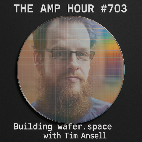
#703 – Building wafer.space with Tim Ansell
Download episode · 81 MB
Also on Apple · Spotify · YouTube · RSS
Show Notes
Welcome back Tim Ansell!
- Tim's past appearances and previous work
- Discussing Tomu on 375
- Discussing Fomu on 456.3
- Discussing the open source PDK on 501
- Tim’s previous work at Google involved releasing a manufacturable open-source PDK (Process Development Kit), which contains the fundamental information needed to create integrated circuits.
- Key open-source tools discussed include OpenROAD (a backend compiler for IC design) and Open Lane (an end-to-end suite turning chip descriptions (RTL) into manufacturing data (GDS)). Andreas had been on the show talking about his work on OpenROAD. Not discussed on the show but after Efabless went away, Open Lane has been replaced with LibreLane.
- Efabless, a VC-backed startup, shut down in early 2025 due to investor disagreements. Efabless previously provided pooled manufacturing access (similar to OSH Park for PCBs) using the SKY130 process from Skywater in Minnesota.
- A Skywater run costs $200k–$300k, which Efabless divided by 40 to reach roughly a $10k price point per slot.
- Tiny Tapeout
- Matt Venn's Tiny Tapeout program further subdivides the manufacturing costs, making it the cheapest way to create custom silicon, typically costing around $300 per design.
- Tiny Tapeout lowers the barrier to entry, allowing people to "just try it and see if you like it," similar to writing a "hello world" program.
- The program has already processed almost 3,000 projects, demonstrating high community demand when costs are low.
- Despite limitations, advanced projects are possible: a developer taped out a Linux capable SOC using open-source tools and the Tiny Tapeout space.
- Introducing Wafer Space
- Tim started Wafer Space, based in Singapore, to provide community access to open-source manufacturing after Efabless ceased operations.
- Wafer Space focuses on the GF180MCU PDK (Global Foundries 180 nm process), which is a much cheaper technology manufactured in Singapore.
- The core offering is a low-volume production run: $7,000 USD gets you 1,000 chips back. This volume is enough for prototyping and shipping a small product (e.g., 500 units).
- The design envelope area is 3.8 x 5 mm (20 mm squared) using the 180 nm process.
- Interested parties should sign up via the Crowd Supply page. The deadline for purchase is the November 28th and submissions are due by December 3rd, with delivery by March 15th.
- Manufacturing & Packaging
- By default, customers receive bare silicon die
- Tim is working with PCB manufacturers (like JLC PCB, PCB Way, Seed Studio) to offer Chip on Board (COB) wire bonding assembly onto custom PCBs (think black epoxy blob on a PCB)
- COB packaging is significantly cheaper (sub-$2) than standard packaging houses (which often charge around $7 per chip).
- This approach also provides faster iteration speed, as PCB manufacturers offer quick turnaround times (sometimes 3 days) compared to typical packaging houses (3 months)
- Getting Started & Resources
- If you are new to chip design, starting with Tiny Tapeout's click and drag tools is highly recommended. Matt Venn previously talked/sang about Siliwiz
- More advanced tools include Verilog and VHDL (coding style) or KLayout and Magic (drawing shapes, similar to PCB design).
- To follow the project or seek help, join the Wafer Space Discord
- New services offering open-source silicon manufacturing include IHP (Europe/130 nm) and Chip Foundry (US/Skywater), increasing ecosystem resiliency.
- Website: Wafer.space
- Sign up on the CrowdSupply campaign
Transcript
Chris Gammell: This is The Amp Hour Podcast. Released September 24th, 2025. Episode 703. Building Wafer Space with Tim Ansell. Welcome to the Amp Hour. I'm Chris Gammell of Contextual Electronics.
Tim Ansell: And hello, I'm Tim from Wafer Space.
Chris Gammell: Hey, welcome back, Tim. How are you doing?
Tim Ansell: Good. It's been a while since we've last talked on the Amp Hour.
Chris Gammell: I know. Yeah, five years or so. Time flies, huh?
Tim Ansell: Yes, it definitely does. The last time we were talking about open source Silicon Space and the fact that I was at Google at the time and we just released a open source PDK that was actually manufacturable.
Chris Gammell: Yes. Remind people what a PDK is?
Tim Ansell: PDK stands for Process Development Kit. And it's basically like the fundamental information you need to create silicon chips or integrated circuits.
Chris Gammell: Yeah, and that was part of your broader push at Google to just do open source silicon. And that really, between that and then like all the open lane that was part of the CIA did some of that stuff, not DARPA. I don't know who was doing open lane, but Andreas was on the show talking about it at one point.
Tim Ansell: Yes, Andreas Olesen was part of DARPA and they did two programs called Posh and Idea. And out of that project came a place and route tool, which is kind of like a backend compiler for IC design called Open Road. And that was then integrated into a complete end-to-end suite that basically let you turn the description for chips, the RTL, into GDS, which is kind of like if you're a PCB person, the Gerbers of the chip design world called Open Lane. So, and that was done by a company called eFabless under contract from Google.
Chris Gammell: Cool. Cool. That is a lot of words there. But I think actually if people listen, they should, some of those should sound familiar, I think. And this is all, you know, like you were pretty fundamental in moving a lot of this open source silicon stuff forward. So it's been good, except we've had a roadblock, not a roadblock, but a setback, I think a couple months, years ago. When did that happen?
Tim Ansell: At the beginning of this year.
Chris Gammell: So tell us what happened there.
Tim Ansell: eFabless was a VC-backed startup. And sadly, some investor disagreements meant that at the beginning of the year, that company shut down. And so eFabless was responsible for making it possible to do actual manufacturing. They were the equivalent to, say, Oshpark in the PCB world. Or if you're too young to remember the world before Oshpark, kind of like PCBWay or JLCPCB or those kind of newer pooling services, eFabless was doing that with a company called Skywater in Minnesota, who did the actual manufacturing.
Chris Gammell: Yeah, that's what's interesting. So we had Matt Ven back on the show like a year ago at this point. And Matt subdivided down one of those, but that subdivided down like a lot of wafers as well, right? So it's like a fraction of a fraction of a fraction sort of thing, right?
Tim Ansell: Yeah. So the way I kind of like to think about it is, you know, doing an actual run to make silicon wafers costs, you know, 200 to 300k, at least with the Sky 130 process. And so if you divide that by 40, which what eFabless was doing is how you get down to about the 10k price. And then Matt Ven would then take that 10k price and divide it even further. So that is how he gets to the $200 price, which allows for 200 bucks. You can basically get your own circuit design manufactured and you get back a PCB board with your chip mounted on it and ready to go. So by far Tiny Tape Out, which is the program Matt Ven runs that does this, is by far the cheapest way to create your own silicon chip. And so like one of the things that I think people don't really realize is that kind of at this price point, it no longer matters whether or not you're doing something useful or whether you really have any goals in mind. You can just try it and see if you like it. A comparison I often bring up when people ask me, what use is this?
Chris Gammell: Don't ask that. No questions, please. We're not taking questions in the audience right now.
Tim Ansell: Well, like nobody asks whether Hello World is useful, right? That's right. Yeah, that's a good way. It's the first step in learning whether this is something you want to do, learning how things work, all these type of things, right? And it takes a lot of work to get to a point when you're a coder before you're doing programs that are actually useful. This is kind of the same in silicon. And Tiny Tape Out really gives you the ability to do that and see whether you like it for a very low cost price.
Chris Gammell: It's probably cheaper than a Lego kit. Yeah, especially those things are getting up there, like the Death Star and all the ones that you can build that are massive, right? So the VC thing, that didn't work out with eFabless. That sucks. But what about just the, you've had this view of the industry, obviously you've been within the industry pushing for a lot of this stuff as well. Aside from the fact that the eFabless is no longer with us, companies are still building this stuff past the Tiny Tape Out stage, the try it out, the hello world of silicon. Now you're moving into the Osh Park, the PCB way, more eFabless, and what we'll be talking about here, your new venture. Like, are companies actually doing this? And then what are they building with it?
Tim Ansell: So I guess one of the big things with open source is it's hard to know exactly what people are doing because unlike with, you know, proprietary solutions, you don't have to ask for permission, right? Like anybody can just decide to do things. But recently, I think maybe it was last weekend, there was Orconf that was actually hosted in Matt Venn's hometown of Valencia. The recordings from those talks are all up. And there are numerous groups there talking about doing open source commercial projects, including a group that maybe I'd recommend you want to get on Ampower. Thomas, who's from Spherical, who is doing basically chips that go into space using completely open source tools to develop basically new types of power supplies for all the type of things that go into space, which seems like a pretty cool topic to discuss with him about.
Chris Gammell: You always give a good list. People are going to be hearing like, and this guest was recommended by Tim. Tim knows a lot of people and it's very helpful for filling out The Amp Hour guest list. So I always appreciate that. Thank you.
Tim Ansell: One of the things that I think is really helpful in the community is like just sharing that there are other people out there doing cool things. I would have never got into this space if I hadn't found out from various other people all the cool things that were happening. I think it's kind of a duty of people to kind of share other cool work that's going on.
Chris Gammell: Yeah, I totally agree. And actually, I've stepped away from Twitter slash X and just a lot of social media generally. And it's just that was a lot of my source of news and how I found discovered stuff like that. So it's like, yeah, you have to, you know, kind of depends on your sources and where you find this stuff. Hopefully people are using The Amp Hour like that. So, yeah, other ways like that. Are there other news sources that you use? I mean, social maybe these days.
Tim Ansell: I do think that the loss of Twitter was a bit of a setback. There's a lot of stuff happening on LinkedIn, but it's a little bit different because of job aspect that LinkedIn has always pushed. LinkedIn seems to be where a lot of Silicon people are hanging out. There's obviously, you know, Blue Sky and Mastodon and Threads as well. But the volume just isn't as high as it was when Twitter was at its heyday. So sadly, I don't have much more than that. There's a lot of stuff happening on Discord, but that's not really a news source, right? It's more like a chat channel.
Chris Gammell: Kind of flies by too. Kind of if you miss it, you miss it sort of thing, which is... Yes. Well, and if people may have missed your new project, which you're here to talk about and I definitely want to hear about. So what is your new thing?
Tim Ansell: Coming back to kind of the eFabulous collapse. At the time, eFabulous was pretty much the only way if you're doing open source silicon that you could get your stuff manufactured in small quantities at a reasonable price. One of the things, though, that I was somewhat frustrated with eFabulous was that at Google, I had released two open source PDKs. There was the Sky 130 PDK, which is 130 nanometer all-inclusive type process technology that was manufactured in the US at Skywater in Minnesota. They're a fairly small foundry, which makes it a rather expensive technology. But we also partnered with a company called Global Foundries to release the GF180 MCU PDK. And Global Foundries is one of the quite big silicon producers in the world. I think they may be in the top five. I was always trying to push them to do an equivalent program for this technology, but they never did. While they existed, it didn't seem right to somewhat create a competitor to eFabulous. But with them kind of disappearing, I kind of decided, well, maybe it was time to make that a reality. And so I started a new company based in Singapore to basically provide the community access to the GF180 MCU PDK manufacturing at a much lower cost because that's a much cheaper technology than the Sky 130. And that's manufactured by Global Foundries in Singapore.
Chris Gammell: That is awesome. Just to clarify on the Global Foundries thing. So your work at Google had kind of opened them up, opened up the Global Foundries thing. But then you're just saying eFoundries wasn't picking up on it kind of thing. Is that the idea? As like a commercial offering?
Tim Ansell: As part of the Google program, we did a couple of free shuttles where we had over 80 different people tape out designs and get chips back. But the problem was that none of those people could really continue to do any development because there was no cheap way to get more chips made. And, you know, eFabulous, obviously, I worked very closely with them and I'm still good friends with a lot of people who were at eFabulous. But they very much decided they wanted to focus on the Sky 130 process technology, which, as I said, is a good technology if you need the features or you need your chip manufacturing happening in the US. But, you know, that drives the cost up. And I am a big believer that the cost is proportional to the ability for people to do interesting stuff. So the more we can drive the cost down, the more people will be able to do cool and exciting projects using the technology. And so that was kind of my focus with doing Wafer Space. It's very much based on how Osh Park operated in the early stage, that it's a basically you give us a design and we manufacture it. There's no kind of support or any of those type of things offered. That's all done by the community. But in turn, it means the price is as cheap as we can offer it. And so what I'm kind of offering at the moment is for $7,000 US, you get a thousand chips back.
Chris Gammell: Yeah, that's not a small amount of chips. What's the equivalent at Skywater? Like, or I guess the eFabulous of yesteryear. What were they doing? So it was like $10,000 for a run, but how many chips would you get out of it sort of thing?
Tim Ansell: Somewhere between 150 and 200 chips back. And I think that's the big difference that I'm trying to do here is that a thousand chips is enough that you can actually think of it as low volume production, not as a prototyping service. Right. And so like with a thousand chips, get a thousand chips back. You do your first prototype PCB run and, you know, mount a hundred chips on that. And it doesn't work because your first version never works. And so you do your second one, you know, you get another hundred and that works. And then you've still got 500 left for the product that you ship to your customer. And, you know, 500 units sold is definitely a very good start for a small product. And, you know, it's seven bucks a chip means these products owe a hundred dollar products based on the, you know, three times bomb cost means you can have kind of like a $30 to $40 bomb. And of that seven bucks being a custom silicon seems like that could work.
Chris Gammell: That is very viable. I work for industrial customers that were like, yeah, we ship in like a hundred units a year, maybe. And if there's a high value arena that they want to lock down a little bit more, really customize, make it super power efficient, you know, that's where this really starts to come in, I feel like.
Tim Ansell: Yep. And, you know, that's kind of what I think is interesting about this approach is as well. It works for things like Matt Venn's project. You know, he charges 200 bucks in many cases, because if everybody got a board back, he wouldn't have enough chips. Whereas with the wafer space offering and a couple of months ago, Matt Venn announced that he was porting tiny tape out to the GF-180 MCU technology, which is what wafer space is offering. He could probably offer an even cheaper option than he does today because he has plenty of chips, right? And maybe even offer you getting back more than one. Today, everybody only gets one back, which means it's good for like experimentation. But if you ever wanted to like build a small product out of it, you know, maybe you only want five or something or even just one to give your friend, right?
Chris Gammell: I was just thinking when I smoked the first one, because I always seem to, you know what I mean? Like you don't have to be as delicate just to move innovation forward, right? Just to speed things up and allow people to run a little looser and closer to the rails.
Tim Ansell: Yep. And I think that's a big thing here is that like, and that's why it's common for industry versions of this to give you maybe 50 chips back at total. And they tend to also have quite strict requirements that you're not allowed to sell them or any of these type of things because they're running these programs at a loss. The reason they're running these programs at a loss is because they just don't have enough people doing chip design. And I think the thing that the open source stuff has really shown is that the reason people aren't doing chip design isn't because nobody wants to do chip design. It's because there are very large barriers to entry and huge costs involved. And so like the open source silicon, I think has really changed that. I believe Tiny Tape Out has done almost 3000 projects through Tiny Tape Out and every run seems to have even more projects than it did last time. And so I think this is really showing that when you open it up and really allow people to experiment and give a cheap way to do learning, there is the ability for people to create enough designs to make this a industry that doesn't have to lose money.
Chris Gammell: Right, exactly. I mean, I feel like you guys should also start a recruiting arm. You and Matt should start like the wafer space slash Tiny Tape Out graduate pool of people who know how to actually build chips good because the industry needs people like that as well.
Tim Ansell: Yep. That was one of the things back when I was at Google was that when talking to the government, they were very clear that they needed 100,000 new designers over the next 10 years, which is, you know, 10,000 students a year. Yet all those programs they were offering were only maxing out at, you know, a thousand people a year, because if I was a employer, I would want my silicon designer to have done some type of tape out as part of their learning. And there was, or in many ways still is, no way to get 10,000 people every year to do a tape out. I really think this, if they're right, and I actually think they're wrong in that I think they've underestimated how many people are needed. I think places like Tiny Tape Out and what I'm doing with Wafer Space have shown to be really the only way to scale up the number of people entering this industry. And I think one of the things that I had in an early day of Google was kind of like a graph which showed that Google's hiring rate of hardware designers. And if you extrapolated it, there was kind of like a point where in something like 2030, Google would have had to hire every single hardware engineer on the planet.
Chris Gammell: Well, obviously AI is going to do it, Tim. Come on. What are you talking about?
Tim Ansell: Well, all these AI run on chips, right? So that's actually one of the things that has been an advantage is that thanks to AI, there is a lot more interest in chips. And like those people are working on some of the most advanced technologies on the planet. But there's this kind of cruel thing that's kind of happened is that all the senior executives learnt on very easy technologies. But today, when a person does their first tape out, it can frequently be on something like a 12 nanometer technology in their PhD program. That being the first time you've ever done a tape out.
Chris Gammell: A million dollar masks and stuff like that, right? It's just like, oh my God.
Tim Ansell: Yep. You get one chance at it. And, you know, people screw up all the time. It's part of being, you know, a human. And so that's kind of a bad way the industry is. Whereas like tying tape out, if you screw up, you know, it's only 200 bucks, right? And hopefully in the future, it'll be even less than that.
Chris Gammell: That's like a textbook cost, right? That's basically one textbook.
Tim Ansell: Yep. Being able to cut your teeth on these older process technologies, which also, you know, are much more well behaved, right? When you get starting to get to these advanced technologies, physics starts to go a bit wonky. You have to worry a lot more about quantum effects and all these other stuff. On these older technology, things are much easier. It makes sense to start there.
Chris Gammell: Well, let's talk about that. So I have your crowd supply page up right now, which is also linked at buy.wafer.space. And we'll link all of this stuff in the show notes, of course. But let's talk about the layers, the size, the capabilities, especially compared to the 130. Because you said, you know, you said there's some stuff in 130 that people don't need. Maybe let's just start with, okay, so there's a 3.8 by 5 millimeter design envelope area. And you have these five layers. It's 180 nanometer process. What is the benchmark for what you could put on there? Maybe at the high end of like really tightly packed kind of design.
Tim Ansell: I've always struggled to answer this question because there's a big difference, I think, between what industry says you can put in this space and what the open source community is showing you can put in this space. The example I kind of give is there's this developer who has created his own Linux capable SOC that was taped out on Tiny Tape Out. He did that entirely by himself, not as a full-time job, as a part-time job. He is an embedded software developer by trade, I believe. I've never met the guy in person. He developed this and then taped it out on Tiny Tape Out. Industry would have said that you don't use 130 nanometer process technology to do a Linux SOC. You can't fit it in something like Tiny Tape Out. Tiny Tape Out is way too small to fit something like Linux capable processor. But I have a Tiny Tape Out board with his design on it and it boots Linux. And, you know, the great thing about it, him being an embedded, you know, software person is like, I want this to boot mainstream upstream Linux kernel. You don't need some board support package or anything. It just boots, you know, you download Linux from kernel.org and compile it and it boots. And so this was all done by one person as well who'd never done, like, it wasn't like he was previously a chip designer or something. I forget when he started, but less than five years ago, he had never done any type of chip design or anything like this. And now he's doing, you know, full Linux capable SOCs through Tiny Tape Out. If you think about it, the 20 millimeters squared is way more space than you get with Tiny Tape Out, you know, because Tiny Tape Out takes that space and divides it by about 100. So you could definitely do something like a Linux capable MCU.
Chris Gammell: Yeah, I think one of the things we've talked about when Matt was on the show was just like limitations are usually going to be like onboard SRAM. You know, you're going to go off chip for a lot of this stuff because you're just not going to have, you know, making a microcontroller versus a microprocessor, that sort of thing. You're going to pack in like memory units, things like that.
Tim Ansell: Yeah, I think that's mainly a performance question because, you know, if you're willing to go off chip, then you can have plenty of SRAM through things like the P, the SPY SRAM that things like the Espressif 32 have made really popular. And that's how he did the Linux thing is that the main memory is stored in a SPY SRAM, which, you know, is a little bit slow, probably much slower than say using, a DDR memory interface, but it definitely works. And so I think that's kind of the other thing to think about is what do you actually need to do your project? I think the other thing is we know if you move something from software into hardware, it can get significantly more efficient. Maybe you don't need that gigahertz CPU if the things dedicated hardware running instead of it being all in software. And, you know, that was something that I kind of learned the FOMU project, which we talked about previously was that like the FOMU has a little soft RISC-V core by default. And I'd say it's how I trick software engineers into becoming hardware people, because you can start by programming that like RISC-V CPU with like embedded C or embedded Rust or even MicroPython, but it's a bit slow, only runs at about 20 megahertz. You know, our software engineers are used to hundreds of megahertz these days and things like this. But you can do things because it's a soft CPU is like if you need to read eight, you know, bits from eight different registers, you could rearrange that. So it's only one read. So instead of it being, you know, 16 instructions of like a read and then an XOR to get out the bits and all these type of things, it can just be in the right place. So that's like a single register read that can significantly improve your performance by 8x. And so all of a sudden that 20 megahertz processor is much more powerful than you thought it was. And you kind of show software engineers this trick and then you go away and you come back and they've developed this whole system, this massive SOC with all this hardware acceleration. And you're like, well, I guess you're a hardware engineer now and you never knew about it. And so then obviously the next step after that is you can convert that into an actual chip now. It doesn't have to stay on FPGA. I definitely still think FPGA is a great way to get started. If you want to go further, you can, and it's no longer as expensive, right? At seven bucks a chip, you know, that's not much more expensive than say an FPGA. And so all of a sudden you can also do things that you can't do on FPGAs, like analog circuits and other things like that.
Chris Gammell: What about how these things are like actually delivered back to people? You know, you're going to be designing these chips. Actually, I was looking at the timeline, which is tighter than I would have guessed as well. So you take final submission date, December 3rd. You expect these to be delivered to customers by March 15th. What would people be getting in the mail on March 15th?
Tim Ansell: So by default, they'll get back bare silicon die. So that is useful if you want to do more processing on the die or you have special requirements. I'm also working with a number of those PCB manufacturing houses to allow me to ship those die directly to those places to be assembled onto your board using a technology called chip on board wire bonding. Instead of getting back a bare die, which most people know what to do with, you can get back a PCB with your chip already mounted on it, ready to go. And that will all be done through these board manufacturing houses like PCBWay, JLC, PCB, Seed Studio, all that type of thing. And that offers you a lot more flexibility.
Chris Gammell: Are they regularly doing chip on board?
Tim Ansell: It's not a standard offering as of today, but that's mainly because people don't normally have a source of chips that aren't already packaged. And so it hasn't made sense for them to offer something that nobody can use. With things like wafer space, the hope is that now there'll actually be customers for this. It makes sense for them to offer that. And we're still working through what that flow looks like. And the reason I'm doing this is because silicon is seven bucks, but it costs you seven more dollars to do the packaging of the chip. That doesn't make sense to me. You can choose to get your die back and work with a packaging house if you want. You're perfectly welcome to do that. But this chip on board packaging means the packaging can be, you know, sub $2. And it also means if you want to, you could turn your die into something like a little dip package, right? Your PCB doesn't have to be, you know, a full product. It could be something like one of the ESP, you know, 32 style modules, or it could be a breadboard compatible, you know, dip pin chip. And another group that we're working with is the group that's trying to make a replacement for the Z80. Obviously, those chips are all in dip packages. And so they want, you know, a design that they can just drop into existing designs. And so they will probably be using a PCB that makes it look like a dip package.
Chris Gammell: Yeah. I mean, at a certain point, it's just a little bit of, I mean, polymide could be also epoxy, right? I mean, it is kind of an epoxy type substance anyways, I think, right? I mean, make your own mold, drop the thing in and there you go.
Tim Ansell: Yep. So I'm not an expert on epoxies or chemistry, but I'm certain you could probably encapsulate them like that if you wanted even the thing to look like a dip package.
Chris Gammell: Yeah. And you're specifically not going towards like a packaging house that would put into a standard QFN or anything like that?
Tim Ansell: The big problem is packaging houses don't want to deal with this size of volume. And even when they do, they charge exorbitant prices, right? As I said, seven bucks per chip is probably fairly cheap from a packaging house, especially at the volume that we're kind of dealing with. And so plus their turnaround time is terrible.
Chris Gammell: I am actually surprised that with all the, you know, the rah-rah, you know, U.S. chip making stuff that nobody has even, as far as I know, I mean, I could be very wrong about this. I have not heard of anyone trying to do U.S. based packaging. Just like, there's no motion in that. I think every time I've asked someone about it, they're like, I don't know anything. You know, it's always going to Malaysia or Philippines or Vietnam or, you know, wherever, it's super high volume. But I just feel like with all the U.S. chip stuff going on, that someone would be like, yeah, the U.S. is going to need this too. You know, like, okay, fine.
Tim Ansell: So there are people doing that. I know Skywater has a play in that space. They're doing advanced packaging. And what we need is like stupid packaging that is super cheap. And that's just not an area that groups like the Chips Act is really focused on. They're focused on, you know, super high-end chips and these type of things. There's probably places in China that would do it for the type of cost and volume that would make sense. But, you know, again, they generally aren't offering it outside of China. I'm hoping some of that will change though, as things like WaferSpace start having people have more bare die looking for bonding services, right? Like one of the things that I would probably say is that there's probably less than 10,000 people out there looking for packaging services today. And you know, every run I do is 40 new people who potentially need packaging services, right? And these 40 people each need a thousand parts packaged. That is 40,000 new parts that need to be packaged. And so the hope is there'll be some of an ecosystem built up around this. But until that day, going with an ecosystem that is already, I think, thriving, which is the PCB ecosystem, makes sense to me.
Chris Gammell: Yeah. And just to be clear on the PCB one as well, is that like the black blob that people would see on like, so like when Dave does tear down and there's like a black blob, epoxy blob that's on the board, that's often chip to PCB kind of style of bonding?
Tim Ansell: Yep. That's exactly that type of bonding. The Tyne Tape Out team actually has a video and a blog post about their first experiment doing that. There's some demonstration of that working already. We just want to make that a regular option that is available. And this is also like why I want to get black people bare die is that they can then choose what they want to do here. Whether they want to go with an expensive packaging house, whether they want to use a PCB house or, you know, wire bonders aren't that expensive. A secondhand wire bonder on eBay can be a couple of thousand bucks. And so if you want to just do it yourself, maybe that's what you want to do. What is it? Have you done that? I've never
Chris Gammell: considered it. Obviously there's not a lot of options out there for me, but like, how can people do it?
Tim Ansell: I know people who have wire bonders. The general experience is being the fairly grumpy machines. This could be again, though, that's the type of thing that if you don't use it frequently, it tends to be grumpy. But if you use it every day, it tends to be really fine. I don't know. But like the idea is that this gives people options. As I said, kind of people having bare die to even like practice on or use these type of things was extremely rare. It definitely hoping that that will change. You know, I'm hoping that people in the community will be like, oh yeah, if you get these wire bonders and use these settings, it will work. Because that also gives you a lot of options. Like if you want to iterate on how your form factor is, like a packaging house will easily take you three months to get stuff back from them. And you know, a PCB manufacturer will get you back stuff in three days these days, right? Like this is a much faster iteration speed if you're doing that.
Chris Gammell: You know, as you're saying this stuff, what I'm really thinking is, Tim says wire bonders are a couple thousand on eBay, but I would say there are a couple thousand on eBay right now. And if this becomes a thing, there's going to be a hot market for a wire bonder, like used wire bonder machines, I bet.
Tim Ansell: Maybe. I mean, even new, they're not that expensive.
Chris Gammell: Oh, really? Okay. I just always assumed it was like this really complex process.
Tim Ansell: Wire bonding, you know, has been around since the 1980s-ish, I think. It's a very, fairly well-known technology. The high-end machines that you know can wire bond a thousand chips a second, and those type of things are obviously significantly more complicated. But I think the low volume stuff has still been around for a long time. Again, not that complicated a technology compared to anything else in the semiconductor world, right? It's interesting. It's interesting that that's a thing that's needed still, you know? Yeah. I think it's again, one of these things that the ecosystem isn't there because of people just don't regularly get this type of part that needs it.
Chris Gammell: Let's talk a little bit about logistics. So first off, everybody should go sign up on the CrowdSupply page to get notified because there is a, as far as I understand CrowdSupply, you need to get
Tim Ansell: like 200 signups before it goes live, right? Yeah. Once it goes live, which should be pretty shortly, you'll be able to purchase the $7,000 slot or the $8,500 slot, which includes the wire bonding. Or if you want a full wafer, we'll also be offering full wafers for $2,000. If you just want a wafer, either because you want to do some more post-processing or because you want a cool looking thing and you've got a disposable income, then sure, go and buy one. Yeah, that should be easy to do. I think we've already got the number of signups needed there. It's just waiting on a few things before we can get that live. I'm guessing by the time this podcast comes out, it will probably,
Chris Gammell: the buy links will already be there. Yeah. I mean, it's not a small amount, but again, if you have someone who's like looking forward or if they're, you know, previously had been going eFabless, it feels like that seems kind of, kind of no brainer, you know? Yeah. And I think the
Tim Ansell: important thing is that the more people who do this, the cheaper it will get. And so, you know, I'm not doing this because interested in making a lot of money or any of these type of things. I'm doing this because I think it's important for people to be able to actually make the designs they have. And so if we get more people doing it, then that price could definitely go down substantially. Because if you think about it, as I said, it's, you know, a rather large number divided by another number. If that other number is, you know, the divided number gets bigger, the actual price goes down. And I think that's also, you know, an important thing to think about is one of the things I give, do you know, FIRST Robotics? Yeah, of course. The high school thing, you know, to be a competitive team in FIRST, my understanding is you need about $10,000. If we had, you know, we were about 25% of the size of FIRST Robotics, I would need to do one of these every week. At that kind of volume, I'm sure the price would be substantially lower. You know, you're talking more like $2,000 to $3,000 per slot instead of the $7,000 slot. And the kind of other statistic I give is, you know, if 50% of high schools in the US submitting one design a year, so that's not like a class thing, that's like an afterschool club type thing. If they were submitting one a year, I would need to run one of these MPWs effectively every working day of the year. And at that point, 30% of the global mask manufacturing capacity would be dedicated just to my projects. And that would drop in cost too, I'm sure, because
Chris Gammell: then it would also, you know, volume goes up, cost comes down, you know? Yep. And you know, that's just
Tim Ansell: the US. That doesn't include anybody else in the world. I don't think we're going to get to that anytime soon, but I definitely think the capacity is there in the same way that people are starting to learn programming and AI in high school. Maybe chip design can be another thing that a percentage of kids in every school is interested in doing. And again, I'm not talking about necessarily it being a required course of that everybody does. I'm talking about, you know, a club that, you know, five to 10 kids at that school want to do something using, in many ways, which is the humans most magical
Chris Gammell: technology we've ever invented. You can sand talk magic, right? Yeah. Yes. I kind of like to say that
Tim Ansell: we hit rocks with lightning and make them think, right? Like it's pretty cool. The type of things happening in semiconductor industry are definitely on the same, you know, technology level as things like going to space and these type of stuff, right? Like as humanity's crowning achievements and the fact that it's kind of all locked up behind, you know, you have to be a billion dollar company is sad, right? Like it should be something that everybody has access to and can do and use and have fun with.
Chris Gammell: So you mentioned like the after-school club, that sort of thing. So what is the latest and greatest on actually like building a design? So is it just Verilog and that sort of thing? Is it magic? What are the tools, the open source tools of the trade these days? If you've never done it before, you
Tim Ansell: know, Tiny Tape Out has developed a bunch of click and drag type tools. I like to say that anyone could get started with a couple of hours on the weekend and get to the stage where they could submit a Tiny Tape Out design. They've had primary school kids do this. The one that Matt always whispers, is that the one? I think there's plenty of examples. I was attending a conference or like an event called Open Source recently and had a little booth there that a friend, John Master was running. Randomly, a person came up, like this young kid came up and he had done a tape out on using Tiny Tape Out and he was, wasn't in high school yet. I have no idea who he is. This class kind of randomly was enough that, you know, a person turned up who had done this. And so I definitely think anybody can get started with that flow and see if they like it. There's no shame in it being not your cup of tea. Like, there's plenty of things I don't like, you know, that you probably like. So give it a go and see if that, if it's something you find fun. After that, you know, there is things like Verilog and VHDL that you can go to, which is much more coding style. You know, if you're kind of a software background, things like Verilog are probably going to be very familiar. And then if you're more like a PCB designer background, are very into like the drawing of things, that's where you get kind of into more analog circuit design with things like K layout and magic, as you mentioned. That's kind of much more drawing shapes on a thing, just like in many ways, drawing shapes on PCBs and that type of stuff.
Chris Gammell: When Matt was on, we talked about the kind of the parallels to like a key CAD or something like it, right? It's just like they do, it does all kind of line up. Obviously the geometries are significantly different, but at the end of the day, it's like shapes on a screen that eventually becomes shapes on a planar surface. And then, you know, you have to learn a little bit more about implant depths and stuff if you're doing really, really analog-y things, but most people will not be doing that,
Tim Ansell: I imagine. Yep. There's these things called standard cells, which are like your AND gates and your OR gates and all those type of things. They basically created a key CAD library of those parts. So you can design in the schematic editor effectively your digital circuit. And so I thought that was pretty cool and fun. And I definitely think there is a bunch of stuff where, for example, a design, like to do the chip on board stuff, you need to design a PCB. So some more integration between the ASIC design tools and the PCB design tools could open up a lot of more opportunities in custom optimization because you don't end up with that thing where, you know, the pin you want to use is on the wrong side of the chip, right? Like I'm sure we've all gone like, screw it. I'll get a higher number of layers in my PCBs because I just can't route this circuit any other way. Well, maybe if the chip had been designed slightly differently, you wouldn't have to do that. And so like, I think there's some interesting things that could happen there. And because it's all open source is that there's no problem for people doing that. Somebody could try and design a silicon circuit in CLICAD. As you said, it's really just shapes. I think it'd be a bit crazy, but you know, I wouldn't stop you. If you submit something that is
Chris Gammell: DRC clean, I'll manufacture it. I can imagine like a case where like someone goes from like, Eric Schlepfer's like monster 6502. That's basically like just a blown up version of a 6502 in actual transistor form. And so you would take that, replace with standard cells, shrink it down, shrink it down, shrink it down. And then eventually, I mean, you might not want to pay to have a 6502 and you could buy one, but you could also add your own stuff in there. That's what I think.
Tim Ansell: Yeah. I think we're seeing that things like Oshpark allow people to do things that, you know, are just cool, like PCB artwork, these PCBs that are like pieces of art,
Chris Gammell: every one of my designs, Tim, is a piece of art.
Tim Ansell: Fair enough. You could do that in silicon if you want. If you have the funds, maybe you've got a grant and want to make a really tiny piece of artwork, go ahead. Again, you know, the industry will say you're silly for doing that, but I won't. I think it's really cool to enable people to do things that otherwise they wouldn't be able to do.
Chris Gammell: That would actually be fun to go to like a gallery and it's just like, it's just like a wafer, or not a wafer, even just like a chip up on a wall. It's just like, everybody has to wheel around their own like magnifiers, you know, in order to see anything.
Tim Ansell: Yep. And you know, there actually is a long history of silicon designers putting silicon doodles in their chips.
Chris Gammell: Yeah, you got to fill that space with something, you're paying for it.
Tim Ansell: Yeah. It would be interesting to see if people with a little bit more artistic talent got in there and did some interesting things. There's a whole bunch of stuff you could probably do with like diffraction and stuff like this. I'm no expert, but it definitely feels like there's opportunities to do fun and interesting things there.
Chris Gammell: Yeah. All right. So first off, silly whiz is the word I was trying to remember. That's the thing that Matt always sings and or whispers. That's the learning tool for analog circuits. So 180 is where we're at currently, Double Foundry is over in Singapore. I mean, does that mean you've had to be over there? Like, have you been able to go to the fab? How has that relationship worked and what does it look like in terms of you working with them?
Tim Ansell: I don't need to be in Singapore myself, although I will be visiting there in a couple of weeks. The actual relationship is mostly just signing contracts and doing all that type of boring paperwork. I do that so that you guys pretty much don't have to. Other than that, you know, there's actually not a lot to do here, which is also why it can be as cheap as it can be, right? Like when you think about it, my project divides this by 40 slots. That's at maximum 40 customers that I have to deal with. At the moment, the kind of cadence we're looking at is once every three months. Dealing with 30 to 40 things once a quarter, you know, it's not that hard. The logistics are actually pretty easy from that size. And like the great thing about silicon is it's really small.
Chris Gammell: You're not scaling up a new factory or, you know, shipping, you don't have to deal with like shipping and logistics of like, you know, big truckloads of things.
Tim Ansell: Yeah. You know, your a thousand chips would probably easily fit in a normal envelope. You know, obviously I wouldn't be shipping in an envelope because you know, you want to protect them, but it's not a large amount of space, even though the number seems quite big. Yeah. Right. The other reason is that I'm doing it in Singapore, you know, is there's a bit more uncertainty at the moment with stuff happening in the US. And so if you're not in the US, having a group outside the US that you can work with, I think is quite useful. And, you know, as an Australian, I'm technically outside the US from that point of view.
Chris Gammell: Right. You spend a lot of time in the US, but you are outside the US.
Tim Ansell: Yes. There's actually a couple of other services that have popped up after eFabulous collapsed. That's kind of the nice thing about open source is that, you know, everything eFabulous had done was proprietary. It would have all died when an investors had disagreements. Right. But with, you know, open source, there's a foundry in Europe called IHP that does a similar process to Skywater. It's 130 nanometer process. You've got me in Singapore, and then there's a new group called Chip Foundry that is doing stuff with Skywater as well. And so now you've got three options to get open source silicon made, which is significantly better than one option we had previously. That also gives you options, right? Like if you need your chips manufactured, say in Europe, you now have an option. If you need it manufactured in Asia, you've got an option. I think that's an important part of building kind of resiliency in the ecosystem. It also, you know, helps to have competition. It means if one group is doing something in a stupid way, the other groups can do it the right way. That kind of thing, I think is also important about this. You know, you had mentioned, you know, we keep kind of
Chris Gammell: calling back to the eFabless stuff. And, you know, one thing you kind of call out on the on the crowd supply page, too, is about the like the IO ring and things like that. And so one thing I'm curious about is just like the kind of the you'd, you know, you said trying to keep the cost low and stuff like that. But the supplementary services of like design checking and IO rings and things like it is, is it as paired back from what people were doing on eFabless as well? Like things that you have to bring, bring themselves or checking they need to do? Or is it just is it just computer checking?
Tim Ansell: It's just computer checking on my side. We definitely will have templates that people can use if you don't want to design your own. I think the community has come a long way since when eFabless first started out. And I think there's also a bit of a difference in that, like the Skywater, the IO cells were extremely complicated. The IO cells on GF180 MCU are a lot simpler. And so we also have tools like pad ring generators that now exist that kind of didn't exist or at least weren't tested when eFabless first set out. So a pad ring is basically the IO cells or the IO pads. Pads are where, you know, the wires are bonded to in wire bonding. And they go kind of around the edge of your chip. And so those affect how you package the chip. You kind of think of it as the footprint in the PCB world. A lot of that stuff has come a long way since 2020 when we first started doing lots of stuff. It made sense for eFabless to standardize a lot of that stuff when there was a lot more unknown and uncertainty there. And that does mean that they could offer, you know, getting you back a PCB board with your chip mounted ready to go, which is something that I'm not offering, for example.
Chris Gammell: Got it. So they tied that into the packaging option then, like the tiny tape up board comes back with like one QFN mounted to a PCB, that sort of thing. But that's because it comes back from eFabless as a
Tim Ansell: QFN, right? Yep. That also drives the cost up and reduces the flexibility. And so that's definitely good for when there was a lot more unknowns. But since the world has kind of become more mature and a lot of the open source tools have become a lot more mature, I think that's less needed now. And I'm optimizing more for cost, I think is a strategy that I'm exploring. Ship Foundry, which is the US based one, is going for a more all inclusive service, is my understanding, which makes it a bit more expensive, which kind of also makes sense because the base skywater technology is also more expensive. The value adding of having that makes a lot of sense. And so like, this is also what's good about having multiple options is that we can explore which one makes the most sense, right? Like, maybe it will turn out that everybody uses the same template with my service, and we want to bring packaging back in as part of the service in the future. I don't know, I've got lots of requests for Beardai. We'll see if those people actually put their credit card into the system or not. That's always the big thing is people say plenty of things. But until they actually put their money where their mouth is, it's hard to know if
Chris Gammell: that is actually a real thing. That's product manager 101 right there, right? It's like, yeah, don't
Tim Ansell: listen to the feedback until they plop the credit card down. Yep. And so we'll see what happens. This is my attempt at doing this. But you know, I'm like anyone else, I'm making it up as I go along. And we'll see whether or not I've made the right predictions here. And I'm open to change as well, right? Like, if this doesn't work the right way, we'll change it until it does.
Chris Gammell: Yeah. Where do you usually refer people, you know, just to kind of wrap it all up so that people are understanding where they should be going if they're hearing this next. First off, where do you refer people if they need some help with stuff, you know, in terms of like getting stuff off the ground, almost like design services in this space? And then if they're doing it all themselves, then what are the
Tim Ansell: the next steps? That sort of thing. I kind of have a thought that goes like this, you know, if you've never done anything before, I think your best bet is starting with Tiny Tape Out. As I said, Tiny Tape Out is currently working on support for GF-180 MCU. Once they've validated that, you'll even be able to move designs from Tiny Tape Out directly to wafer space. That's not ready yet, but coming in the future. If you've done a design before and just want to start making your own chip, then I recommend either joining the wafer space discord or the Fosse chat element. Either of those methods will get you into a community that has a whole bunch of people doing stuff in that space. There's also a number of companies that are offering commercial services. If you want to pay somebody to help you do designs, people like Chip Flow or MyBrains are happy to offer basically paid support. Wafer space itself doesn't offer any paid support.
Chris Gammell: Did you say MyBrains? Like, I need to get this chip idea out of MyBrains under the silicon?
Tim Ansell: I, for a long time, called it MA Brains, but apparently it's MyBrains. They did a lot of work on the Omba Source tooling and in fact are behind a bunch of the stuff that was done to get the GF-180 MCU PDK out there. And so they're very familiar with that. I definitely think we're in early stages, so there'll be a lot more as people do tape outs. I'm working with a guy called Leo who is doing a lot of things like the examples and the pad ring. Those will be available shortly as well. As well, as you said, sign up for the crowd supply to be notified because as the campaign goes along, we will definitely be sending out updates with more information on examples. One thing we do have is that because there were two Google shuttles that had run previously, we do have at least 80 designs that have been previously manufactured using this technology.
Chris Gammell: And those all had to be open source too, right? Wasn't that a requirement of the free shuttle?
Tim Ansell: Those basically provide an example of what can be done on this technology and would definitely work to highlight some of the coolest ones that you can use as inspiration. I'm slowly getting around to updating the website with that. And probably again, by the time this is posted, there'll be some more stuff on the website in that area. Yeah, that's great. I think that you say you can do
Chris Gammell: anything to me and it's just like, I'm like, I say, okay, I do nothing. But if you start showing like examples, it's like, oh, I can modify this to be a little bit different there. You're creating a new sensor or a new processing element around it. I can maybe use that in a different space. Those kind of examples are super useful. And yeah, that's great. You continue to push the field forward and I'm really appreciative of it. I'm not taking the jump myself, but hopefully someday in the future, I'll hold some silicon I designed in my hand. Because like you said, it's increasingly accessible. I'm never a bleeding edge kind of person, but I'm right in the middle of the curve. And I feel like that curve is catching up to me real fast.
Tim Ansell: Yeah. And like, as I said, it's 200 bucks and two hours on the weekend to like do your first design. And like, as I said, don't worry about the fact that you don't know what you want to do or any of these type of things. Just jump in and work through the examples. If all you do is submit a thing that, you know, does the sample output, which I think is like outputs your name on the LED, you know, 200 bucks. I'm sure as you, as I was saying, like, that's a piece of Lego, you know, it's not an expensive Lego kit. It's more of the lower end Lego kit, right?
Chris Gammell: That's a cocktail party story right there too. I mean, you bring this thing, you know, of course you bring your circuit boards with you to a cocktail party and then you'd be like,
Tim Ansell: hey, look, I designed this. Something to keep on your desk, right? Like that you can show off. You know, I think somebody like you, two hours is perfectly reasonable to get that hello world out there. It's not a thing like, um, Matt Venn teaches a course quite frequently, a live course, and most people are able to submit something to be manufactured by the end of that course. And the biggest blocker I've seen is people just going, you know, oh, the thing I'm doing is, you know, trivial and these type of things. Everything somebody does at the beginning is trivial. It doesn't matter that like, that's how you learn, right? You do something trivial and you keep doing it until somebody turns around and go, hey, wait, that's no longer trivial, right? Like I'll challenge you that by the time I'm on the next Ampower, you've done some of your own silicon.
Chris Gammell: Yeah, that's fair. That's fair, man. I like it. I like it. Challenge accepted. Great. Especially because I'm in charge of scheduling. You're like, Tim, you can't come back yet. I need to do, I need to spend two hours on the weekend. Yeah. All right. Well, Tim, thank you once again for being here. Wafer.space to check out Tim's latest project. Check it out. It'll take you to CrowdSupply to sign up if you're interested. Looking forward to talking to you next time and having a design in hand, of course, because I have to. Cool.
Speaker ?: Cool. Cool. administered administered administered administered administered administered
Global FoundriesOpen SourcePDKSilicon ManufacturingsiliwizSkywaterTiny Tapeoutwafer.space
Keep current
Every episode, plus the occasional job post, in your inbox.