
#469 – An Interview with Craig J Bishop
Download episode · 77 MB
Also on Apple · Spotify · YouTube · RSS
Show Notes
Welcome, Craig J Bishop!
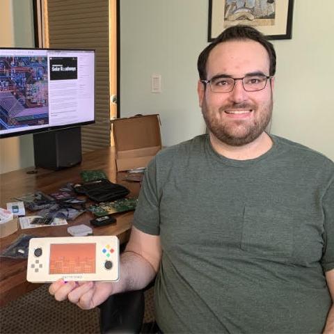
- Craig designed and built the Gameslab, which is a custom gaming platform built with a Xilinx Zynq part (XC7Z035). (Update: Craig has been posting more about the Gameslab on his site here)
- Bought reballed chips on PCBs. They were actually a $1200 chip he got for $80.
- Episode with Ryan Cousins
- There is apparently a kit for counterfeiting Xilinx chips
- National lab has a pdf on how to detect counterfeits
- Digilent Zybo
- Craig built the board on the JLC 6 layer process at 210x100 for each board. $150 for 5 PCBs.
- DDR3 chip was .8mm pitch
- Using stack up to calculate impedance/prop delay
- Used an excel sheet to track delay and skew for nets, since KiCad can't track delays between layers
- FPGA on chip delays are also stated in the datasheet and need to be accounted for.
- Running Rust on STM32L0, on kernel modules in A9, applications / games
- Sense resistors with instrumentation amps going to the ADC to measure each rail's current draw.
- BQ24250 chip for charging with configurable registers
- Zynq doesn't necessarily need the bitstream programmed first. Instead the A9s boot first and can load the bitstream.
- Every game brings its own hardware
- Can put the Gameboy hardware into the fabric!
- Craig doesn't like verilog, so he uses a higher level language called SpinalHDL. It is a fork of Chisel, which is based on Scala.
- Each of the above languages are strongly typed. Loosely typed means you can convert between data types, like in C.
- "Verilog is becoming the assembly language of FPGAs"
- ZipCPU
- AXI bus
- Most designs need to reimplement different hardware blocks. But there are libraries in Chisel, which can implement things easier.
- Vex Risc V
- Created a frame buffer for the LCD and some 2d graphics acceleration on the Gameslab.
- Learned to program to make PC games. This was part of the idea behind the Gamesphere project as well.
- PIC18F452 in a 40 pin DIP
- Used AT91R4000 for the game sphere
- Andrei LaMothe wrote the book "The Black Art of video game console design"
- Cypress dual port SRAM
- Craig's first "big boy job" was working for a a neighbor up the street starting a semiconductor packaging company (Tim Olson)
- Deca Technologies was opening a Wafer Level Chip Scale packaging fab in the Philippines.
- After iphone came out, there was a lot of demand for low profile complex chips.
- Raspberry Pi photon problem
- Added a "squishy" layer to the silicon, and then exposing certain parts of the silicon to the interconnect.
- The graphics problem was that they wanted to make the chip bigger but the silicon smaller
- EWLB from Infineon looks like a plastic wafer.
- Can put two chips next to each other
- There was a paper about the subject (has the image Chris and Craig were discussing during recording).
- Sometimes the parts are placed 30 microns to the left, which is not good for the substrate they are placed upon.
- Can get really expensive PnP machines but they go slow.
- The microscope would spit out X, Y and rotation, but it scales with chip complexity, such as when there are two chips.
- Needed to do traces between them
- Craig's job was to take the output and do some autorouting between them.
- Feature sizes were 1 micron
- Package design looks like PCB design
- Cadence sells System in Package designer but is really Allegro with different plugins.
- Can people do their own SIP?
- Craig thinks that design will move towards more SIP
- Split die architecture
- Split it into a few pieces: This will help improve yield and flexibility, as well as modularity.
- Chris asked about Chiplets, a topic that is championed by Dr Subu (sp?)
- Chiplets are going to do interconnect in silicon, not plastic
- Example is BLE and micro
- Adaptive alignment
- Craig gave a talk at KiCon about how Autorouters work and how they have been improving.
- Not your grandpa's autorouter
- Freerouting is nice and available but it's not the latest
- TopoR
- Moving towards interactive design (P&R), but Craig thinks it should go the other way.
- Generative design would be better
- Dave Vandenbout's SKiDL talk
- Craig was briefly interviewed by Piotr and Alvaro at KiCon
- Find Craig on his personal site where he is documenting his projects (craigjb.com) and also find him as @craig_jbishop on Twitter.
- Check out the Phoenix 3H (hardware happy hour) if you're in the area!
Transcript
Craig J Bishop: This is the A-B-R-Podcast, released December 1st, 2019. Episode 469, an interview with Craig J. Bishop.
Chris Gammell: Welcome to the Amp Hour. I'm Chris Gammell of Contextual Electronics. And I'm Craig Bishop of Mango Dynamics.
Dave Jones: Hey, Craig, how you doing? Pretty good. Good, Chris. It's almost Thanksgiving holiday here in the U.S., so we're having a nice, easy, pre-Thanksgiving, pre-gorging ourselves talk about electronics and everything else. Yep, I'm fasting. Yeah, you mentioned you have a couple Thanksgiving dinners to prepare for, so it's good. It's good. It's a problem when both families are in town.
Chris Gammell: Yep, yep.
Dave Jones: So we got to hang out a little bit at Supercon, and I asked to come on the show. And I'd love to talk about the thing that you had in hand and then kind of work back to what you've worked on in the past. So what were you showing me at Supercon?
Chris Gammell: All right, so at Supercon, I had a large thing called a game slab wrapped around my neck, which when I received the official badge for Supercon, I looked at it. In fact, I hadn't looked at it before, and I found out, hey, that's an FPGA badge. And I haven't worked with the open toolchain, so I don't know how fast I could get something running on that. But I brought this giant thing based on an FPGA, so why don't I? My friend Tom Shucker, who was there, just said, why don't you put that around your neck? Yeah, just add a lanyard. That's the badge now. Right, and he had a kit with zip ties and everything to kind of add a lanyard to it, and hung it around my neck, and it was heavy, but much easier.
Dave Jones: Two years later, you got a sore neck and a lot of questions about it. Exactly. So now let's do a little disambiguation here. Is it games lab, or is it a game slab, or both?
Chris Gammell: So you could say it's both. Originally, I wanted it to be game slab, because it's very slab-like. Yeah, it is. It's pretty beefy. It's over an inch thick, and it has a 10-amp hour battery on it. Yeah. Which, at the time, I thought it was gratuitous, because the FPGA turned out to take a lot less power than I thought. But for Supercon, that ended up working perfectly, because it lasted all day. Yeah, fewer charge cycles. Yep.
Dave Jones: So what is on this thing, this game slab? Slab of games.
Chris Gammell: So it's got a Xilinx Zinc FPGA arm Cortex A9 combo. So the story behind that is, for years, I've been wanting to build a handheld console based on FPGA. And I've been looking at Zinc parts, because they have a nice dual-core arm built in. And on eBay, there's all kinds of chips you can buy on eBay. I heard someone at Supercon call them, you can buy chips on tape, you can buy chips on real. And on eBay, you can buy chips on PCB. Which, like a lot of sellers on there, cut these chunks of PCB out of used electronics gear with an expensive chip on it. Yeah.
Dave Jones: They don't even do the work for you of removing it and reballing it and stuff like that?
Chris Gammell: Well, it depends who you buy from. So a lot of times, you'll see, like, literally in an eBay picture, you'll see a roughly cut-out chunk of a PCB with a Vertex 7 on there, which is a $10,000 chip. And they don't want to risk it before they sell it to you. So they'll just sell it to you on the PCB.
Dave Jones: They just use a Sawzall or something? I don't know.
Chris Gammell: That's crazy. Some guy with a Dremel tool cutting these down. Yeah. Oh, man. Hopefully a mask, too. I found this seller. I think it was Jia Xungtong Chip Co. Something like that.
Dave Jones: Might have to get a link for that later. Yeah, we'll see. Unless you want to hide your source, we can always bleep that out, too.
Chris Gammell: Oh, yeah. Uh-oh. He actually took them off the PCB and did the reballing for me. So he was selling them already reballed. But he's a part about it, too.
Dave Jones: I think that's important. Yeah. It's not like, oh, these are new parts. These are definitely reclaimed chips.
Chris Gammell: Yeah. Well, I think the term they said was refurbished.
Dave Jones: Yeah. That fits the eBay aesthetic, right? Right.
Chris Gammell: Gently used. I was still very skeptical. But if you look on eBay, so this is the XC7Z035, which is a really big zinc part. And if you look on DigiKey or Avnet or Mouser, it's like a $1,200 chip. Which, of course, their pricing is always high in onesies and twosies. Sure, sure, sure. Especially for FPGAs. But still, not cheap.
Dave Jones: Yeah, probably still a couple hundred bucks in quantity kind of chips, right? Exactly. These are not commercially viable chips. Or not going in your consumer goods, rather. Yeah, yeah. No. No kidding. Not in your games lab. Maybe a Snickerdoodle or something. Yeah, right. But... Right, yeah. So we should say Ryan was on talking about similar parts a couple episodes ago, Ryan Cousins. And that was the Snickerdoodle. But I think that was a much smaller part, too. So less FPGA fabric. It still had the A9 cores, but less fabric around it.
Chris Gammell: Yep, yep. No, I had a lot of fun listening to that. And yeah, so this is a much bigger chip, which I only got because of this eBay guy. So probably a year ago, I found it on eBay. And I saw the price. It was... I think it was 80 or 100 bucks or something like that per chip. And I impulse bought five of them because I was like, I'll find something to do with these if they work.
Dave Jones: Yeah, definitely.
Chris Gammell: But I was still super skeptical about them actually working or not. Because I read a lot about counterfeit chips, especially big chips like that, where you can take another chip and like Dremel off the markings or... Yeah, right.
Dave Jones: Just re-silkscreen the bigger chip's name or something like that.
Chris Gammell: Apparently, it happens all the time. So Xilinx plastic LQFP and DQFP parts. Apparently, there's whole companies that sell kits for taking... You Dremel off the top layer of plastic with the markings. And then there's actually this epoxy that you put on top of it to mask that. Oh, my gosh. And then you re-silkscreen it.
Dave Jones: I mean, really, that's a sign of just how much money there is in doing this counterfeiting because that there's kits to do that kind of... Like, that's crazy.
Chris Gammell: It's like hilarious to me. And I found the... Maybe we'll have to link to that. I think it's one of the national labs, I think, has a PDF going through all the ways to identify possibly fake chips. And they have tons of Xilinx examples and other expensive chip examples in there.
Dave Jones: Actually, yeah, that sounds like a great resource.
Chris Gammell: Oh, it's hilarious, too, because you have to look for signs of sandblasting. Wow. Wow. Yep. Anyway, so I got the five of these, and they arrived just fine. But in order to actually test them, you can't just power a few pins and throw a JTAG on there. It actually requires pretty much a whole board to be able to test it.
Dave Jones: Yeah, because FPJs always have, like... I think they've gotten better. But I remember they used to be, like, you have to, like, bring power supplies up at the same time. And you have to have, like... You know, it's a significant amount of current, too. Even at the... Especially for the low... Like, the 0.9-volt rail... Right. You know, things that are going to the core.
Chris Gammell: Well, it turns out that the sequencing is not as catastrophic as it could be. Because I've messed that up a few times, and it still lives. Oh, that's good. But the power draw still is a big problem. And not just that, but the thing has tons and tons of power BGA. It's got BGA balls on it, so... Yeah.
Dave Jones: How big is this part as well?
Chris Gammell: What is the BGA count? So, it's a 676 ball part. But it has a really easy pitch. It's a one-millimeter pitch.
Speaker ?: Yeah. Okay.
Chris Gammell: And so... And before this, I had been working on a Zync dev board just playing around. So, I had a bunch of software and a bunch of FPGA stuff ready to go. I just needed a board to try these out. And so, I decided to try to figure out if I could get a board for this part without spending $1,200 on a PCB as well. Right. And that's how...
Dave Jones: So, not a super high layer count kind of thing. Not super... I guess the pitch was good to start with.
Chris Gammell: Yeah. Well, if you look at things like... What was it? A Digitalant Zybo, I think, was the board I was using?
Dave Jones: Yeah.
Chris Gammell: That's one of their... Yep. Yeah. I think it's an 8 or 10 layer board. And I didn't really feel like paying that much just for a board to figure out if these parts worked at all.
Dave Jones: Right. Yeah. Although, I mean, 8 and 10 are getting cheaper, but not cheap. Right? Yeah. I'm guessing you were trying to get to like JLC 6 layer type of thing, right?
Chris Gammell: Well, that's exactly where I ended up, actually. Because JLC 6 layer is the cheapest out there by far now for 6 layer iPhone. I think these are...
Dave Jones: They're cheap on a lot of things.
Speaker ?: Yeah.
Chris Gammell: Yep.
Dave Jones: I mean, quality too. Like, you know, like, yeah, quality. But like, I think the pitch you need and yeah, everything. Yeah. It sounds like it was a good start.
Chris Gammell: Well, it turns out the two key things were... So, it was a 210 by 100 millimeter board, I think. And it ended up being about 150 bucks for 5, which is awesome. And the key things were the 6 layers and that they would do a stack up that matched the impedance for DDR3. Yep. And then also their via diameter was small enough because the DDR3 chip is a 0.8 millimeter pitch.
Dave Jones: Oh, I see. Okay. So, even though the FPGA was okay, the memory was more challenging.
Chris Gammell: Yeah. Yeah. And so, I should eventually publish my blog post about that. But figuring out that the impedance and the right stack up for the DDR3 routing on six layers was interesting because it turns out that if you use the top and bottom layer on the JLCPCB 1.2 millimeters thick stack up, then you get a pretty nice microstrip that gets you somewhere close to 50 ohms, which is still above the 40 ohms for DDR3 that it's in the data sheet, but it's close enough and it's just one chip, so it should work. And then to use an internal layer, it changes the impedance and then also changes the propagation delay. So, this is where I learned some fun tricks in KeyCAD, or I guess fun tricks combining KeyCAD into Excel, because it turns out, so KeyCAD has length matching, but when you're routing a high-speed interface like this, you actually want delay matching.
Dave Jones: Right. Yep.
Chris Gammell: And when you have traces on different layers, internal and external, they have different delays for distance traveled.
Dave Jones: Right. So, if you need to hop between layers, you're saying it's difficult. Yeah.
Chris Gammell: Exactly. So, I had this... Challenging. Yeah. Yeah. Yeah, exactly. So, I had this giant Excel sheet with length on layer one, length on layer three, length on back layer, and it would multiply out by the delay on each layer. And then it would calculate the skew for every net. And then it would show me whether those skews are within the spec or not. And then I also had to... So, these FPGA parts are so big, they actually have a delay on chip, too, before the signal gets to the BGA. And so, you also have to throw that delay in there.
Dave Jones: Or how do you... Is that just like a spec thing?
Chris Gammell: Yeah. It's kind of annoying to get. You have to go into the vendor tool and have it spit it out for you. But it gives you picoseconds delay. It doesn't give you like a length because the length is not what matters.
Speaker ?: Right.
Dave Jones: Yeah. I guess even the length, you're really trying to get to the delay as well, right?
Chris Gammell: Right. Right. Right. And I think Kikad eventually will have delay length, delay-based matching. But right now, it just has length-based.
Speaker ?: Yep.
Dave Jones: Okay.
Chris Gammell: So.
Dave Jones: Well, so you got through that, it sounds like. I mean, like it's... So then what was the boot up process like? I mean, how did you validate what was going on?
Chris Gammell: So, the first thing is after I got our first board back. So, the board has DDR3, the Zinc, a USB transceiver. And let's see, it has some power management stuff. Like there's a STM32 on there for managing the power sequencing and battery. And then there's a TI battery management part. And once I got it back, the first thing to check out was the power supplies, which I like using Rust now for all my embedded firmware development.
Dave Jones: And Chris White just had an aneurysm. He likes to poke fun at him. But yeah. Yeah. Okay.
Chris Gammell: We'd love to hear about this though, yeah?
Dave Jones: Yeah. Yeah.
Chris Gammell: Which we can talk about that more later. But it's been a great experience so far. Yeah. And so, I loaded minimal code to bring up the switching regulators and try to get the sequencing right. And that's where I mentioned, if you get the sequencing wrong, it doesn't seem like things blow up. Yeah.
Dave Jones: Spoken from experience, it sounds like. Right.
Chris Gammell: And then once the power supplies are up, the first thing I do is throw a JTAG debugger on there to see if it even sees the FPGA. And more key, see what part it says it is.
Dave Jones: Right. Right. Oh, yeah. Yeah. Because that's what you were trying to get to in the first place, right? To validate this is actually what you bought. And so. Just real quick on this. So, you were running Rust, and like you said, we'll talk about this more later, but you were running Rust on the A9 on board. Is that right?
Chris Gammell: So, Rust is running three places on here. It's running on the SDM32 that's running all the power management and the battery management. That thing's an L0, so it's always on. And then it's also running in kernel modules in Linux on the A9 because when you put custom hardware in the FPGA, you have to write drivers and stuff for it. Yep. And writing drivers in Rust is still not fun, but it was an experiment.
Dave Jones: Sure. Yeah, it sounds like this whole thing is a playground for you, right?
Chris Gammell: Yeah, basically. And then the applications, the games are also written in Rust and user space. Oh, cool. Okay. So, everywhere possible.
Dave Jones: Great. I mean, this is your party, man. You get to play with how you want. Right. I didn't quite get that. So, when you said SDM, you said at SD part doing all that stuff. So, you meant it was actually a supervisor micro on there. Yeah. Is it built into a broader power management chip or is it separate from the power management chips? And then the SDM32 is actually talking to those chips over I2C.
Chris Gammell: So, I looked at some integrated power management, but I actually really wanted, since this is just an experimental thing, I really wanted to try Rust. So, I wanted an ARM part, and then I wanted to monitor all the power rails separately. So, I have a current sense on all the power rails and voltage sense and current voltage sense on the battery. Because I had no idea how much power the Zinc chip was going to take for different workloads. So, I really wanted to have everything on there to be able to monitor that.
Dave Jones: That's great. I mean, the L0 chips are SIP power and, you know, they're, yeah. So, you just have like an external instrumentation amps around like a sense resistor or what?
Chris Gammell: Yeah. So, there's, I think, five sense resistors on there. And each of them has a fixed gain amp on it going into the ADC. And then there's, I think, one of the rails has a voltage divider to get it into the range of the ADC. Yeah, that makes sense. And then, oh, it's one of my favorite parts. It's a TI. I should look up the name of that part. BQ24250, I think.
Dave Jones: Yeah, it's definitely something BQ2400 family, right? Yeah.
Chris Gammell: Because that's all the charging chips, yeah. And it's a two-amp charger if the system's not running, but it switches the system load between the battery and the adapter automatically. Uh-huh. Ah, that chip is amazing.
Dave Jones: Yeah, those things are great. I mean, they just kind of, they don't just work, but like, and they have like control registers, and a lot of them have control registers now too, right? So, you can do some configuration stuff in there. But, that's cool.
Chris Gammell: I was actually really afraid of that chip at first, because I hadn't done battery management stuff before. So, I actually built a separate board first to prototype just that, and ended up being completely unnecessary, because it worked out of the box. So, yeah, I highly recommend those chips. Not cheap, though. Yeah, yeah.
Dave Jones: No, no, they're not. They're like four or five bucks, right? Exactly. Yeah. Well, again, this is a playground for you, so that's, if you take the game slab, you know, to product, I think a lot of things will change.
Chris Gammell: My supply chain needs some work.
Dave Jones: I'm not going to make it to, I'm not going to make it, I'm going to say it's not going to make it to the market. What are your plans there?
Chris Gammell: Yeah, not as is. Yeah. Even eBay pricing, the $80, $100 FPGA is still a little bit bomb busting. Yeah, it definitely is.
Dave Jones: Okay, so you got this thing up and running. That's great. And then, so then the JTAG was to, so you had to get the JTAG chain up and running to even talk to the A9, is that right?
Chris Gammell: Or is this to talk to the rest of the FPGA? Yeah, so the Zinc parts actually are different than other FPGAs, that they don't necessarily go out to a bitstream flash first. They actually boot up the dual Cortex-A9, and that ARM part of the chip actually controls bringing up the FPGA side. So you get JTAG access to the ARM side first, and boot up the ARM processors, and make sure those work. And then from there, you can do whatever you want to boot up the FPGA fabric. And so in my case, I worked out getting the debug UART to go through the STM32 over USB, creating a firmware for that. And then after I had debug out, then I worked on putting Uboot into the boot flash. So that way, the Zinc would boot up Uboot bootloader, and I had to port that. And then once you have Uboot, you can actually think about booting something like Linux. And that part actually ended up being okay, because I had already tried all that on the Zinc dev board. And it was just a bunch of fiddling with configs and stuff to get it ported over to the new board. Yeah.
Dave Jones: So the Uboot, you had to, so Uboot was, was that in, any of those steps were in logic, or were those all software still?
Chris Gammell: So that's all software. And then the logic piece is, so the Zinc has no graphics output or anything like that built in. It doesn't have a built-in GPU or anything. So... You gotta build that, silly.
Dave Jones: Come on.
Chris Gammell: Yeah, exactly. What are you doing here? So the idea with the Game Slab is that every game brings its own hardware. So... Yeah.
Dave Jones: Which is similar to how the Supercon badge was too, right? That same idea of...
Chris Gammell: Yeah, exactly.
Dave Jones: ...portability. It's a cool idea, for sure.
Chris Gammell: Yeah, that was really cool. And you could do it, a custom game brings its own graphics hardware exactly suited for its needs. Or I thought with the Game Slab, which I started working on, if you want to do like a Game Boy emulator, instead of emulating the Game Boy in software, I just plop a Game Boy CPU and graphics hardware into the FPGA fabric. And it kind of becomes a Game Boy instead of emulating one.
Dave Jones: That is super fun.
Chris Gammell: Yeah.
Dave Jones: Yeah.
Chris Gammell: So I actually started working on it.
Dave Jones: What does that look like? I mean, what is the Game Boy hardware? I have no idea what it looks like.
Chris Gammell: Oh, so I have a series of blog posts on that, at least a work in progress. And it's a funky Z80 that custom developed by the, I think it was Sharp that made it for them. And the funkiness is that it has an extra instruction set with a prefix that's all the bit manipulation instructions, which were used for a lot of graphics effects and stuff. And it's a single, it's in order, and it's not pipeline. So it's a really easy processor to try to implement in the FPGA. And it only runs at like four megahertz, if that.
Dave Jones: Yeah. It's amazing what they did on those. I mean, the things that I spent so much time on in my youth. It's like, you know. Oh, yeah. Pretty simple processors. You know, they're so cost optimized, all that stuff. But like they did so much with them.
Chris Gammell: Oh, yeah. Well, and all the secret sauce is in the graphics hardware that goes with it. The sprites and the tile maps and all that.
Dave Jones: Yeah. So this is the blog post, starting slab boy. Is that right?
Chris Gammell: Yeah, that's the one. And that was kind of. So when I'm doing this FPGA stuff, especially on the experiment, like games lab, I really, really don't like to write Verilog. So I'm trying to switch entirely over to an alternate HDL. And my favorite one is called spinal HDL.
Dave Jones: Which is kind of. So if people couldn't tell here, Craig is a software minded person who likes to take the barrier. Like for me, I'm like, whatever is the most documented, most easiest, whatever the most people have done so I can look something up on Stack Overflow. It sounds like you're like, nah, I'll just figure it out. So why? Why?
Chris Gammell: Well, it's kind of like I do enough stuff for work and now consulting that, you know, it's very well documented and has to work in production and stuff. So when it comes to this side project, I want to use everything experimental and see what happens. And a lot of times I actually find stuff that I end up using in actual work.
Dave Jones: I mean, it's really no, like, it's very noble and awesome and, you know, like experimental that you're doing all this stuff. I just, I can't imagine myself doing that. That's really, that's, I can't empathize with you, Craig. I'm sorry about that. But it's awesome. You're a little crazy, but it's like the right kind of crazy. You know what I mean? Like, it's like, that's super cool.
Chris Gammell: It's a stay up till 3am because this compiler doesn't support the one specific flag you need. It's crazy. Yeah.
Dave Jones: Yeah, totally. I've definitely done that. Which, I don't know. Okay. So what is, what is, so you said spinal, spinal HDL. Is that right?
Chris Gammell: Yeah. So huge shout out to Charles Popon. Popon. I don't know how to pronounce that, but he's a guy, I think in Switzerland or Austria, somewhere over there that created spinal HDL, which started out as a fork of chisel, which is the Berkeley hardware description language. And they're both based on Scala, which is a programming language running on the Java VM. And I know that's a long chain, but basically it means that it's a strongly typed hardware description language built in a full programming language. So Verilog is kind of its own thing built just for hardware description. And it's kind of a rather limited programming language with a lot of capability to describe hardware. And it's also loosely typed. So Verilog, like the canonical example is, oh, I'm going to assign this 32-bit bus to one wire. And Verilog says, okay, no problem. Versus a language like chisel or spinal HDL, you'll get an error when you try to, when you try to synthesize that telling you, hey, you're trying to connect two buses that don't fit together. You probably don't mean to do that. Tell me what you actually want.
Dave Jones: Okay. And so I don't actually know what strongly or weekly typed means. What does that mean?
Chris Gammell: So weekly typed is kind of a programming language concept that's been applied to hardware description languages. I don't know how well it fits, but basically, for example, if I have a integer that I can't just turn an integer into a floating point number without some kind of conversion in the middle. So like C would be a loosely typed language. For example, I can cast anything to a pointer and I can cast that pointer to whatever I want, do whatever I want.
Dave Jones: Right. You got to kind of keep the structures in your head almost, or well, I guess you have to state them somewhere. But at the end of the day, you're manipulating data. You know, a char is a byte is a, you know, whatever, right? And it's all, it can be converted. You're saying that does not the case in loosely typed?
Chris Gammell: Yeah. So loosely typed languages, that is the case where, you know, a char is a byte or is a float. Sure. Whatever goes. And Verilog is like that. So, and this can, it can be good because it can actually help development speed and let you do things and see that you can't do otherwise. But when it comes to designing. It's going without the bumpers on though, right? Yeah, exactly. And designing FPGA hardware is hard enough already. So adding that complexity on top of it, where if you mess something up because you're tracking all these wires in your head and you connect two buses together and you forgot to put a converter or a MUX or something in the middle and it just silently does it anyway. And then you're stuck trying to figure out what it is.
Dave Jones: Usually there's a warning buried in the 550 other warnings that I had.
Chris Gammell: Well, 500 of those are warnings you just ignore every time anyway. Right, right, right, right. Yeah.
Dave Jones: So, so what about like a VHDL? Isn't that more, I mean, that's more explicit at least. I don't know if that fits the strongly type thing, but VHDL is very complainy. I know that from my past.
Chris Gammell: Yeah. So I'm pretty sure when I say this, that VHDL is strongly type. Someone will probably correct me, but it is way more verbose.
Dave Jones: Totally. Yeah. You got to say, you got to basically like state it in three places and make sure everything matches and it'll, it'll give you lots of, it'll, it'll talk your, you're off.
Chris Gammell: Right. So someone at Berkeley a while ago, I don't know exactly, went Goldilocks on this and I don't, I want strongly type, but I don't want to, to verbose. So they went and created their own VHDL called Chisel, which was based on the language Scala, which is strongly typed, but it's also really flexible. So you can basically create your own language within an existing language. And they created, they called it a domain specific language and they created Chisel for describing hardware. And the coolest thing is kind of like the other popular new HDLs is it spits out Verilog or VHDL. So whatever you write in it, it just spits out Verilog that you feed into all the tools you already use.
Dave Jones: Got it. So this is like the, my HDL, LightX, my gen, all of these other tools that are out there that are starting in Python and, and going to something else. Exactly. It's like a layer above a layer. Yeah.
Chris Gammell: Yeah. I think Verilog is becoming like the assembly language of FPGAs and stuff. So that way we don't directly deal with it most of the time, but you want to know it for debugging and stuff.
Dave Jones: So. That's interesting. That's interesting idea actually. Cause is, is there a layer below Verilog? I mean, there is, right? Cause all the, when they're synthesizing. Yeah. Right. Yeah.
Chris Gammell: Yeah. Yeah. And that seems like even further below and maybe it's analogous to when you compile code, you know, it takes your code and it creates a abstract syntax tree and then goes to machine code. So there's a few layers there too. So maybe it's analogous.
Dave Jones: I don't know. You know, real FPGA programmers program the registers themselves and you know, they, they push their own bit streams that they've hand coded. Right. I write my values for my lookup tables by hand. Exactly. Yeah. Someone out there is nodding their head right now and they, they, they shouldn't be, but they probably are.
Chris Gammell: Yeah. Well, real, real FPGA guys calculate the timing delay on every wire themselves. So. Yeah. Right. Yeah.
Dave Jones: Well, this is, no, it's interesting. So like how big of a project, like, is this pretty, is this pretty niche still? I mean, like what's the.
Chris Gammell: So spinal HL is gaining, except gaining acceptance. Like people at Supercon mentioned it, which is great. So it's not some super niche thing. Um, and it has big followers like the guy who does zip CPU. I forgot his name, but awesome guy that writes all kinds of tutorials online and has all kinds of stuff about formal verification. But he's also a big spinal HDL fan. And I think the reason a lot of people like it and reason I came to it is that a lot of stuff that you don't want to write, but you need, for example, an AXE bus. So AXE is the bus standard used a lot in FPGAs, at least by Xilinx. And it's a complicated bus protocol. It comes from ARM and it has a lot of stuff you have to get right. And if you're doing a Verilog, you have to do all this complicated logic. And then they tell you, oh, use our bus verification model, which kind of probes your thing in a test bench to make sure it's working correctly and does all these checks. So it's a huge pain versus in spinal HDL. They have the concept they stole from programming land of a standard library. And you just import the AXE bus and you import an AXE slave factory and you sell it. Hey, I want to register on this bus at this address. And I want this line of that register to go to this LED or something. And so it takes all that verbosity and it uses this already verified standard library to allow you to create peripherals very quickly.
Dave Jones: Yeah, that's great. Wow.
Chris Gammell: So I don't like writing.
Dave Jones: Yeah, that library idea is interesting. I mean, like, does Verilog has like modules, but I guess do they not have libraries? I don't actually know how that would work.
Chris Gammell: So there's a lot of stuff out there for Verilog. A lot of it's for money or, you know, people develop IP. And then a lot of times you can find code for AXE slaves or masters, but it's not modular enough to, you know, include wherever you want versus the power. It's not just like call it and you're done. Yeah. Well, I think that's kind of the big power of using a full programming language to create the harder description language is that I can use everything in that programming language, like the for loops and if statements and everything to kind of be a meta layer. So I'm writing a program that generates hardware. So for example, the AXE bus, instead of just describing one specific AXE bus slave, I'm writing a subroutine that takes in parameters like what you want and then generates the AXE slave based on that. So probably the best example is the same guy who created Spinal HDL is also behind VEX risk five, which is an amazing implementation of risk five. And when you get the project, you can turn on and off all these different parameters. Do you want a memory management unit? Do you want floating point? Do you want vector? And it generates a whole different CPU depending on what parameters you put in.
Dave Jones: It's like a pull down menu for CPU generation. Yeah, basically. It's a what do you want? And it'll give it to you. Yeah, yeah. Order. You have it your way. Right. And people have been doing this.
Chris Gammell: And like with Verilog, people create all these Python scripts or Tickle scripts, Tickle scripts, which, ugh.
Dave Jones: Yeah, I say Tickle. Yeah. Yeah.
Chris Gammell: To generate Verilog based on inputs and stuff. But then now you're adding this whole other layer of complexity versus something like Spinal HDL. It's all one language. So it's really easy to shut it all together.
Dave Jones: Yeah. And I do like that idea of like, you know, like the benefit of libraries too is like, yeah, sometimes there are bugs in libraries. That is not an uncommon thing. But if you have libraries, you have people just looking at it over and over and over again. You just get reused to the point of, you know, you get more eyeballs on it. You can get more. Exactly. Proof in the field kind of thing. So that is, that sounds kind of great.
Chris Gammell: Yep. Or like a really good example is in the Spinal HDL standard library. There's a clock domain crossing standard library primitives. Oh, yeah. Which is really hard to get right. Otherwise, in FPGA, there's kind of subtle problems. So that's just a standard library piece you can plop down and now you cross clock domain safely.
Dave Jones: Yeah. Yeah. My favorite was always going from like, like, why do they have 33 megahertz? And then I'm like trying to go to 50. It's like that division does not look good. You know, like, and there's much weirder than that too. But it was just, you know, that one always stuck out to me of like, you know, just weird, weird divisors and stuff like that.
Chris Gammell: Right. Well, and like I said before, it'd just be one mess error or not even error, a warning message and a sea of 500 other ones.
Dave Jones: And that's right. Right.
Chris Gammell: But it just don't work, you know? Yeah, exactly.
Dave Jones: So, yeah.
Chris Gammell: Yeah.
Dave Jones: So, well, okay. So, so all this, yeah, you're using this to generate the thing. Uh, and then, so what is inside of one of the examples that you're, so I guess you're doing a game boy type of thing, but like, what else are you creating in there? You're also creating other types of peripheral hardware or what?
Chris Gammell: Yeah. So the one I had running at super con was a frame buffer for the LCD, which ended up being pretty simple peripheral. Cause it just has to kind of count out data from memory onto the screen. And then it also had some 2d graphics acceleration. So instead of the CPU having to copy all this memory around to draw graphics to the screen, I create some hardware that you feed it a command list. So draw this graphic at this position on the screen and with this color being transparent and it's a list of these in memory. And then the hardware goes through that list in memory and fetches that memory and draws it to the destination, like the frame buffer for the screen. And because it's in hardware, I can do things like operate on eight pixels at a time. So it becomes a lot more faster than the CPU.
Dave Jones: Huh? That's great. Yeah. And is this the kind of stuff that would be normally in like a accelerator engine? Like how did you, how did you know to go and structure it like this? Did you kind of borrow from something else or just come up with it on your own?
Chris Gammell: Um, well, the architecture I wanted to experiment. So I kind of came up with that on my own, but it's inspired by like how 2d acceleration work, or at least used to work for a standard PC. Like when you draw a window on the screen, usually your OS tells the graphics hardware, Hey, draw this rectangle from this place in memory to this place in memory to put the window on the screen and the hardware takes care of that. Cause it does a really fast, they called a bit blit from back in the days when you're moving bits around.
Dave Jones: Hmm. Yeah. I'm still real shaky on how all the graphics stuff works. Like I, I talked about it with Sprite when there, I think it was Sprite and maybe, uh, so then when they were on the show during Supercon, but like, I'm just still, yeah. I, I, how did you, how did you go and pick that kind of stuff up? Like, like, did you used to do stuff with the software hardware side of things for PC hardware or what?
Chris Gammell: So back when I was a kid, I learned to program when I was a kid because I wanted to make video games.
Dave Jones: Okay.
Chris Gammell: So I, my dad brought home up the visual basic six step-by-step book and the rest is history. But, uh, I learned, I always wanted to make video games and I would play them and I was more fascinated by how they work than the actual game. And at some point.
Dave Jones: That's a, that's a, that's a healthy, uh, that's a good way to change your, you know, uh, your time from making income to spending income kind of thing, you know, game designers make income game players don't make as much income.
Chris Gammell: Well, eventually it turns out that going in the games industry is maybe not the best idea. Oh, it's tough.
Dave Jones: Yeah. It's a tough, it's a tough place. Yeah.
Chris Gammell: So, um, but I always wanted to make games at least up until a certain point. And so eventually if you're a real game programmer, you learn C and you write your games in C. So learn C, which not a very friendly language learning as a kid. Cause like the loose typing we talked about. And, uh, so learn how to do that with this. I forget what book it was, but it kind of did tile maps and sprites and kind of the similar stuff that you'd have on the old style game systems. But eventually I think this was middle high school. I got, and I had been playing with microcontrollers and stuff like that. Cause back then, uh, microchip and app mail and all these companies did free samples, which is amazing. You just send them a request and you get chips in the mail from wherever.
Dave Jones: Right. Yeah. You want to get something done. Yeah. Yeah.
Chris Gammell: Yeah. So I got a, I wanted to, I was like, okay, I know C now and I've written C on some microcontrollers. How do I write, how do I create my own game hardware now? Because I'm, I want to actually do what the game console developers do and actually write games on consoles. And at the time that was really hard because Nintendo doesn't want you creating games for their hardware. So if you want to do that, well, create your own hardware, I guess. Or yeah.
Dave Jones: Yeah. I later found this is, this is the project where you made the game sphere. Is that right? Is that what we're going towards here?
Chris Gammell: Yeah. So, uh, that was before that I made like a microcontroller based black and white TV game console where it had, I think a pick microcontroller generating the NTSC black and white video signal. Yeah. That's great. That was cool. But, uh, I really wanted to create, what was that using to do that? Uh, so if I remember it was a pick 18 F four 52. Which I think was the biggest I could get in a 40 pin dip. And at the time, so it was on a breadboard and it had very carefully timed assembly loops to spit out the NTSC signal. And because black and white didn't have a color burst, you could do it with just, uh, I think three bit DAC made of resistors. Oh, nice.
Dave Jones: Oh, nice.
Dave Jones: And so this is, this is not what became the game sphere though. This is something prior to that.
Chris Gammell: Yeah. So prior to the game sphere, I was a kid playing around with NTSC video signals, which not fun, but as the TV I had at that point and generating, which you got, you know, well, I'm creating HDMI out of a microcontroller, which exists at the time, but that was, that was complicated. Not something I could have done. Um, but so at the game sphere, I decided, oh, I don't like NTSC. So I'm going to try to create VGA and then convert VGA to NTSC. The game sphere was actually built with, uh, another arm microcontroller. It was a free sample from at mill and that was a 80 91 R 4,000 or something like that. And I was actually inspired this guy, Andre Lamothe, which anyone who wanted to be a game developer as a kid will recognize the name. Cause he wrote all the books about game development. Okay. And he wrote a book called the black art of video game console design. And it was amazing as a kid. Cause it's basically like a, a half of a bachelor's in electrical engineering and one half of the book. And then the other half of the book is how to design game consoles based on that.
Dave Jones: Wow. That's awesome. It's still an amazing book. Is it still in print or no? I think so. I think so. Okay. Yeah. We'll put in the show notes for sure. That sounds like, that sounds like a kind of book where you like, you hand it to like, you know, a niece or nephew and you're like, Hey kid, go learn yourself some, some electronics, you know, and then come back in five years and they're like you, you know?
Chris Gammell: That book was a goldmine, especially written by a guy who he has a huge history of writing game development books and wrote games and ran a game publication company and stuff. And he, you get this book from him. And as a kid, you're just blown away because he shows you, Hey, you can actually make a game console.
Dave Jones: Yeah. Why stop at software? You make the whole damn thing. Exactly.
Chris Gammell: And, uh, some of his videos online, I had seen, he was using this particular app mill chip because it's one of the last app mill arm parts that has a fully external bus on it. So the 256 K of internal SRAM, and then it had an external bus that you could hang whatever you wanted on kind of like the old retro CPUs.
Dave Jones: So it's still a microcontroller because it has internal memory, but you can get at it.
Chris Gammell: Well, and I had peripherals on it, but it has giant external bus, which was amazing. Yeah. That's great.
Dave Jones: And, uh, I had probably signal integrity nightmare, but you know, it's probably not
Chris Gammell: going that fast. How fast is it going? So I ran that part at a hundred megahertz, which was another awesome thing. Yeah. Yeah. That's pretty fast. Yeah. And then let's see, there was a flash chip off of it. And then another part, which I guess started the habit of using expensive parts because it was a Cypress dual port SRAM for the frame buffer. Okay. And that's, I think like a $50 part or something like that. Yeah. Yeah. Wow. But it was a free sample. So why not?
Dave Jones: That part. Well, the why not is if you blow it up and you can't get a second sample, but I guess, you know.
Chris Gammell: Well, they send you a three. If you told them, yeah, there you go. There you go. Yeah. Yeah. And just keep requesting free samples over and over and over. Right.
Dave Jones: Right. Did you, did you come up with a different company names and are you, are you in their database multiple times?
Chris Gammell: I think I used the high school email address that no one ever used.
Dave Jones: Yeah.
Chris Gammell: Nice. It worked. It had EDU. So, you know, that worked.
Dave Jones: Yeah. Yeah. That helps. Well, this is great. And you, so you said people are still calling you about this thing too.
Chris Gammell: Yeah. So I, I get emails and messages online all the time from what I assume are university students doing final projects asking me if I can send them schematics and, or I can send them the design files.
Dave Jones: And do you just send them the picture of the wire wrap board that you made? Cause that, that should be enough to, that's enough to scare me off. That's for sure.
Chris Gammell: Oh yeah. You've mentioned signal integrity. Well, uh, 17 year old me did not know about signal integrity. So this thing is a rat's nest of wires.
Dave Jones: I mean, sometimes it's better not to know, honestly. Exactly.
Chris Gammell: It mostly worked.
Dave Jones: Yeah, exactly.
Chris Gammell: And, uh, this is a great post. I'm pretty sure a lot of these are final projects and that they're politely try to tell them, well, I actually don't really have schematics for it. So even if I, even if I did, I'm not sure I'd give them to you then either, but.
Dave Jones: Right. This is kind of, kind of your job to do the, do the hard work. Right. So it's funny.
Chris Gammell: You just don't get that.
Dave Jones: It's nice to know what the project lives on.
Chris Gammell: Yeah. Somewhat. And, uh, but Hey, that project did have a really important effect on my life because it directly led to my, well, I guess you would say second job, but first big boy job, which was, it turned out that my neighbor up the street, and this was right when I was about to go to university neighbor up the street was starting a semiconductor packaging company as you do. And it just got, you know, everybody has that neighbor. Really? Yeah, exactly. I didn't expect it in our neighborhood, but it was cool. And he came down and, uh, cause my dad and him were sharing a beer and he's like, Oh, what's this? And wanted to see the game sphere. And he started talking and he told me he just got 120 million in funding to go start the semiconductor packaging company. Cause you know, fabs are expensive. It requires a lot of money. Yes. Yeah. Yep. And he's like, I have a graphics problem and I think you could solve this. Okay.
Dave Jones: And that's just, I mean, Craig, I think people are listening are convinced that you are a very bright person. And, uh, it sounds like as a high schooler, you are a very bright person, but it takes a special brand of crazy to then talk to a 17 year old high schooler and say, hello, I'd like you to fix my problem please with my 120 million dollars i i owe a lot to this man tim
Chris Gammell: olson yeah brilliant guy and you're exactly right he has the right kind of crazy and he found a kid crazy enough to say okay yeah right right which that's awesome back is absolutely nuts i had no idea what i was doing or getting into anything that's that is fantastic so what were you getting into tell us so deca technologies that he was starting they were building a factory in the philippines and then with hundreds of million dollars of fab equipment and they were building what at the time are still used i think in a lot of stuff called wafer level chip scale packaging which i learned all this at the time is brand new to me i'm like oh it doesn't have pins it's not a dip or an lqfp or what is this it's not even a qfn how do you hook this thing into a breadboard exactly but it turns out in modern phones like iphones and samsungs and that wire bonds so like if you think back to probably university or something they teach you about chip packaging and they show you these tiny little gold wires going from the chip over to the pins they just have a big problem that they're really thick like their z height is really big they take up lots of room and also they're inductors exactly exactly and so those went away a long time ago by the way so anyone who still thinks in wire bonds you are kind of behind except for well i mean packages are they're still they're still there right there's still a thing but you know when they came back for a while for doing it for chip stacking and because through silicon b is really expensive so you just do a wire bond instead oh really you go like around the edge yeah you do like a little chip sandwich exactly they do these weird things where they take a big chip and then stack a smaller chip so the die pads are both are exposed and then if you get really fancy they do this thing where they stack them back and forth and they actually wire bond in the little cavity between the two chips yeah it gets crazy so what what year is this too like what year is this roughly 2010 okay so this is after iphone came out and everyone every company who's at all involved in the cell phone business is trying to get them and so they came up with a new type of package called a wafer level chip scale package or wlcsp and
Dave Jones: this gets rid of all the wire bonds yeah that's the one that people are going to recognize like oh that that really tiny one that's terrible oh exactly soldering or if you remember on the raspberry pi when
Chris Gammell: it was light sensitive because the one chip was just like a die on the board that's a wafer level csp it's a huge photo inductor your photo uh diode yeah yeah the whole substrate of my chip is a photo
Dave Jones: diode that's right although it was like xenon bulbs wasn't like certain type of bulbs that really did it yeah i forget exactly like a higher energy yeah photon input but still like yeah it's but ground bounds with photons you know kind of thing right but that was that was the whole idea of the
Chris Gammell: package though is you get rid of everything so they make these things they literally take the wafer from the fab like tsmc or ti or wherever it's coming from and they don't cut it up and so you take a whole wafer and then you go to a packaging fab and there's no wire bonders or anything like that there's a bunch more equipment that looks kind of like semiconductor fab equipment very close and you put a couple more layers of metal on it so you create like polymer insulator and you create little vias and you create a couple layers of copper routing and the whole job of the the traces on this is to take signals from the chip out to solder balls and the solder balls are put right on top of the wafer so you at the end you get a wafer covered in solder balls and then finally you cut it up into
Dave Jones: little chips yeah that's crazy too i mean like what is what are the relative thicknesses you know so like you have a silicon wafer probably that's less than a millimeter i don't even know anymore what
Chris Gammell: coming in it's probably 500 microns or thicker and usually they grind them down so the final chips are probably a few hundred microns it depends and then and then you're saying that then they stack
Dave Jones: some other some other layers like a mechanical this is effectively like a mechanical layer right above
Chris Gammell: that you basically have the incoming wafer from the fab and we put a squishy layer of polymer on it and then the copper routing and the whole job of the squishy polymer is to kind of translate between the mechanical properties of silicon which is very stiff and brittle and the mechanical properties of your circuit board and the solder balls also help with this because solder is a little bit squishy like it can be
Dave Jones: it's a little bit ductile so when you're more ductile but now the no lead thing you know yeah
Chris Gammell: and so when your phone heats up and cools down repeatedly as you use it or you know take it to cold weather hot weather the pcb inside has a pretty relatively high coefficient of thermal expansion so it expands and contracts quite a bit at least compared to silicon and so if you directly connect silicon to that then you'll crack your silicon as your pcb expands apart yeah yeah so the goal is to kind of buffer between those two and that's what the package does but now you have competing constraints that i want the thinnest possible package but i still want to absorb that stress so that was kind of the start but where i came in for the graphics problem was an extension to that technology which is hard to explain without talking about that because what the goal was we want to take the wafer level csp and make the package bigger without making the silicon bigger because silicon's really expensive and the problem with the wafer level csp is i can only
Dave Jones: fit so many solder balls in the size of a chip right so let's do some some uh i guess some simple math here right so if it's like a two millimeter by two millimeter square yep and you have uh like one
Chris Gammell: millimeter pitch oh that'd be huge for this like let's say like it's huge for that right okay so
Dave Jones: like what 0.5 millimeter pitch then you still only could what fit four across right is that right yep yeah four across in either direction so that'd be like a 16 bin pga right yep um and so now you're saying that they want to shrink it down to a one millimeter by one millimeter chip and so you'd only be able to fit an equivalent of four solder balls on there right and that would be not good exactly well
Chris Gammell: and it's kind of the competing interest because you have the chip makers that if they can shrink the silicon that's amazing economically but on the other end their customers are designing these pcbs and if you shrink the pitch on me or shrink the solder balls you made my life way harder and more
Dave Jones: expensive that's right right and not to mention spins and everything else right exactly and i have to
Chris Gammell: do high density interconnect on the pcb and i have to you know buy really tiny vias like laser drilled vias
Dave Jones: and all kinds of stuff yeah right it adds up fast yeah especially if you're churning out millions of like this is high volume oh yeah phones and commercial stuff anyways right yep so the this guy's at infineon
Chris Gammell: uh i think in 2007 2008 they came up with this technology called ewlb and there's all kinds of acronym soup in this industry but basically the idea was that when i get the wafer instead of just putting my layers right on top of it then i'm going to cut it up and then i'm going to use a pick and place machine just like for pcbs and take all these dye and put them in some double-sided sticky tape on a steel plate and i'm going to leave a little bit of a gap in between each chip and then after i place them all on this double-sided sticky tape i do an epoxy mold across all of them and it creates what looks like a plastic wafer with a bunch of chips stuck in it and the top surface is flat yeah and then once i have this plastic wafer then i put it into my wafer level csp process and i build polymer and copper layers and put solder balls on it and cut it up so i end up with a bunch of chips that are have silicon dye kind of embedded in it and a bunch of plastic around that that kind of artificially makes the chip bigger without using more silicon oh so it's a so the the plastic wafer is a structural piece you're saying yeah so these chips it's kind of we'll have to link into a picture that uh it literally looks like a wafer and then it has a bunch of rectangles in the wafer that are the silicon
Dave Jones: and then how does the uh how how are the pads exposed on the silicon than the chip itself so there's a couple
Chris Gammell: the whole gets yeah it's gooped you know yeah there's a couple of ways so on the the ewlb kind they the die pads on the chip are actually directly exposed so they they stick those into the sticky tape so then when you mold over the thing and pull off the sticky tape all those connections are exposed and you build on top of that and then there's another method which the company i worked at did deca technologies they did uh where you on the wafer before you cut it up you build some little copper posts on all the connections and then you stick those in and you mold on top of that and then you grind and expose the copper got it so there's all kinds of ways to do it
Dave Jones: right right so it's basically like it's almost yeah it's like you're saying it's it's basically making like a pcb process now where you're now adding so like the copper post you're talking about effectively like vias yep i mean there's always vias there's vias in silicon too obviously there's you know these are just things that happen but wow this is yeah this is really nuts and so so again this is to so you're adding this like plastic passivation layer to add structural strength and to make it a bigger thing yeah then the idea is that you're basically spreading out the pins to match
Chris Gammell: a larger pitch part so you can't you can't really spread out the the pitch of the die but the idea is that if i make the area bigger where i can put solder balls because now i have this flat plastic extension of my chip so i can fit more solder balls on my package and then the other benefit is now my chip is contained in plastic which is kind of squishy and buffers me from stress yep and then also which is a really powerful thing is i can put two different chips next to each other and then when i create this plastic wafer i have two chips next to each other and i can actually route copper wires or traces in this case between those two chips and create two chips in one package ah okay so this starts to get
Dave Jones: into the the surface it was soms or what are they called uh yeah like system package yeah sip yeah so so yeah i had always assumed that those were still doing bonding but like you said earlier
Chris Gammell: nobody really does wire bonding anymore it's it has its niche uses but it's for mobile like phones
Dave Jones: and stuff it's way way too thick got it okay so it's a height height issue and uh it's just not
Chris Gammell: yeah they're not gonna mess around with that well and electrically it's it's not fun either when you're doing like high speed memory slow everything down exactly and so the big problem though is when and this is a problem the industry struggled with because and it kind of held back the adoption of this technology is that when you pick and place these chips onto the sticky tape the the pick and place doesn't place everything exactly where you want it to go ah okay now we're getting back to the graphics problem yeah and so you end up with like oh that chip was supposed to go here but it's 30 microns to the left and 10 microns up from where it was supposed to go and come on guys geez 30 whole microns well yeah you laugh but uh a die pad is typically 50 to 70 microns oh no i know i mean yeah i used to
Dave Jones: work on very small kind of things but like you know it's it's it's all relative scales right i mean we're going from you know things that we can see with our eye down to things that we can that are very very very very very very small so exactly i know it matters and uh so you could fix this problem
Chris Gammell: which one way the industry experimented with and some companies do this is that you buy really expensive pick and place machines they go down to oh so they're super accurate yeah exactly like two microns but the other problem is those go really slow so you have to buy lots of them if you want them to keep up with your factory yeah and so tim the guy who hired me didn't want to do that and so he decided that i would rather buy really fast machines and buy a few of them because if you have to buy lots of machines it capital cost adds up really quickly and they have to make up that over
Dave Jones: all the chips so your chip cost goes up he only had 120 million and that could actually take it you know you need a factory and workers and everything else oh yeah yeah you know like picking places can't be
Chris Gammell: 100 million of that it's too much oh yeah we actually calculated out once that i think to do approximately one way for a minute we would have had to spend 32 to 50 million dollars on just pick and place machines oh my god it was insane yeah so his idea instead was well what if we just measure where they went and then create a new pattern that matches where they went wow so the idea was we take the wafer we take the plastic wafer after we mold it and then we put it under a metrology system like an automated microscope and for every chip it measures its x y and rotation away from where it was meant to go and then the idea was we we feed this into feed these offsets into this black box of software that then spits out a new pattern that matches those rotations and offsets
Dave Jones: okay and and just as a reminder you're doing this as a high schooler or i yeah near to college person i
Chris Gammell: i didn't do so well in college mostly because i was spending all my time working on this
Dave Jones: never let my uh my schooling get in the way of my education huh
Chris Gammell: yeah i mean it was a lot of fun though i learned so much stuff from it and it really jump-started
Dave Jones: everything in my career so wow so okay so so you so you do have to do these transforms but it's like does the metrology equipment spit out some kind of like outlines or what was the output that then you
Chris Gammell: used to actually do the the mathematical translations it would give you the x uh x offset from where it was designed to be the y offset and the rotation and then the software would take those and first it would figure out am i even in a valid range because if it went too far we had no hope so we had to check that first and that's like you just throw that one away then if it's too bad yep there'd be a yield loss and then the goal was not to have too many of those so yeah and then after that we had one method where if you're just putting one chip in a package all you have to kind of do is take some of the wiring patterns and offset and rotate them to match so you take the vias and you move them over so they hit the die pad on center again instead of being off floating somewhere else and then you take all the little traces and rotate and move them to match as well and that works for one chip but then as soon as you have two chips or for some other reasons really big chips then things get complicated because i can't rotate and offset one pattern to match two chips right and so that's when we had to create a system for actually auto routing between these two chips on the fly oh he said the magic word yeah what was
Dave Jones: that on like a peewee's peewee's playhouse or something like the alarm goes off or you get like
Chris Gammell: gack dumped on you or something like that you know yeah no i'm the crazy auto routing guy i was at keycon the crazy guy who likes auto routers yeah yeah i definitely want to talk about that and see in a few minutes here too so the whole idea was that now for every chip we would auto route between the two chips because they'd have some random combination of offsets between them and we needed to create traces between them and then once every chip gets its unique pattern there might be like 5 000 of these on a single plastic wafer then we send them off to a the lithography tool which for those of you listening like you're thinking wow how'd you create a unique mask for everything well the answer is we we didn't use a mask that's right it was a maskless lithography so we just feed in a new pattern for every wafer and so every 30 seconds we generate you know 5 000 new package lithography patterns and send them out to this lithography equipment that would draw them on the wafer yeah this is kind of crazy
Dave Jones: too so it's at the lithography level what is like the feature sizes we're talking about here too sure so
Chris Gammell: at the time it was i think the lithography had a one micron resolution but you couldn't make lines that small i think the lines are like 15 and then 10 micron line in space was solid i think we could we proved we could go down to five micron line in space if we were really careful yeah so this is
Dave Jones: interesting too because you know this is at the chip level but it's actually like from my mind it's like you are literally doing like pcbs you're doing very very tiny etching of pcbs oh absolutely yeah yep and and it's you know it is lithography but it's basically you guys are pulling together the the layout process and the gerber generation you know quote unquote of course right gerber generation in this case is the data files that then get pushed to the lithography which is then pulling
Chris Gammell: in the fab process yep um yep and this is really it's it really is like a pcb design process because um so fab design for front-end chips you have so many constraints like orthogonal only metal lines and all that let alone all the device constraints and for package design it really looks like a pcb design in fact i always laugh because so cadence sells this cad tool that you use for it called system and package designer and it's actually cadence allegro which is the pcb tool just rebadged with some extra features for package design oh yeah so it really is pcb design just with smaller sizes and you have to use cadence allegro so that's yeah well it's its own thing yeah well and actually uh high density pcbs they actually use the very very similar build-up process too in the fab to manufacture them so oh okay all right yep they both use electric so it's just kind of all merging right yeah it's really
Dave Jones: blurring together now yeah how accessible is like so like if okay so i decide i wanted to go and put two two chips onto a package in a sip type of thing how much money do i have to knock on the door with and how like are there even firms that will do this from a like a on-demand kind of design thing there
Chris Gammell: are actually uh so i used to know the names of some of them but you can find them it's mega dollars so and then if you're going to do the the kind of technology i'm talking about generally the first question is you know are you apple or are you samsung so yeah right people actually need it right i mean
Dave Jones: that that makes sense yeah but i can imagine that you know at some point in the future as as topologies not topologies as feature sizes everything just keeps shrinking yep there are going to be non-apples not probably you know chris camels but like non-apples that are at the point where they need to do something like this where they're like yeah we're just buying the die and
Chris Gammell: making our own sips because it's better i absolutely think that's the future i think we're going to get to the point where we stop putting solder balls on these things because it just becomes the whole system because i get rid of this whole intermediate step of going from a die to a package to a pcb board and i just go from a die to a system in plastic basically yeah so and that's already started to happen like the apple with the apple watch that module in there uh-huh they're basically uh leading the charge in this direction that they want to get rid of everything that's not uh super relevant to actually connecting these die together yeah and it's kind of crazy because if you think about it when you or i guess i think about it but when you have two packages sitting on a circuit board next to each other and you have connections between them you're going from a 14 nanometer transistor to a 70 micron die pad to a thousand time bigger like 15 micron trace on a package to a 0.5 millimeter pitch bga to a 8 mil trace on a pcb and then going back down that stack on the other side that's right yeah yeah that's a great point you're probably going through a you know a million divide and multiply by a million in terms of size on each side yeah and it's like and it's and it you
Dave Jones: could say well why not just put all the silicon together then but then you start to lose the interoperability in this you know and obviously that is happening right so you know yep so c's keep getting crazier and crazier yeah but if you need flexibility if you need to be able to swap things out the access to chip design is still even more remote you know like just the yeah well megadollar
Chris Gammell: there's a few problems too so first is designing an soc is really expensive so even if you're using a lot of pre-built blocks it's still probably a 50 100 million dollar endeavor if you're doing anything size you know decent enough size and then also as your chip gets bigger your yield goes down so you're kind of competing economics there right yeah that's a great point yeah because you're saying
Dave Jones: so and this kind of plays back to the the chip size shrinking that often happens during like a cost down phase in the chip designer right where they want to use less space they can drop the price they can get more efficiencies and then like you're saying higher yield because you know variabilities when chris the former etch engineer messes something up and everything around the edge of the 300 millimeter wafer is no good anymore we still get 70 of the wafer to be good but the the larger the atomic piece on that dot on that that wafer the fewer than that the more likely that that larger piece might be
Chris Gammell: messed up exactly yep yeah and so that's why at the cutting edge big companies are exploring things they call like split die architecture so they take what was oh interesting formerly a monolithic soc so one piece of silicon and they split it into a few pieces and they do it for yield they also do it for let's say on your soc you only have so much design resources so one year i spend my design team working on improving the processor and then maybe next year i work on improving the sensors or the radio or something like that if i have only one die i kind of have to synchronize those based on my tape out of the whole die but if i'm using two different die i can have those design teams operate very independently
Dave Jones: as long as they agree on the interface in the middle yeah that's right and they and they do not use uh lithography that is on the on demand it is large max sets that are very very expensive yeah prototyping costs are getting more expensive yeah exactly yep yeah i have been reading about i think uh it was ee times article about chiplets and stuff like that is that kind of the same the same realm of what we're
Chris Gammell: talking about here yeah so uh one of the big guys in that space uh dr subu he talked at a lot of the i triple e conferences he talks about chiplets and he's famous for showing the where one whole wafer is actually one device so it's a it's one chip that's the size of a wafer wait what is the what the hell
Dave Jones: is that so what he does is like a 12 inch wafer like a 300 millimeter wafer or what i think it was a it
Chris Gammell: was a 12 inch wafer and they manufactured all these chiplets so all these die that were memories cpus you know other specialized things and they bond them all onto this giant wafer and the giant wafer is basically an interconnect between all these chiplets and oh so they're doing interconnect now on silicon instead of like what you're talking about in plastic yeah but so his idea is you know oh i'm approved that we can make a giant system out of all these chiplets but then it turns out you know most applications cannot afford that if you're not like some military radar or something so then that's where other technologies you know like instead of using silicon i can use cheap plastic and connect these
Dave Jones: together got it i got it so that's like basically them saying we could do it and this is the best way to do it but you're saying yeah but it's cheaper if you do it the other way yeah it turns out a lot
Chris Gammell: of things out there that people want to build care about cost so yep yeah same here i'm a cheapskate man
Dave Jones: yeah great um so what does this look like then okay so let's get back to the actual so you're doing an auto route now yep between let's just say we're gonna have our example here is going to be can we say a processor and a d-ram is that sure realistic or what does it what does it look like
Chris Gammell: between the two does it or like i think one of the ones we did was a microcontroller and a ble chip and it was right when ble was exploding and they didn't have time to integrate a ble so like i have my die from the microcontroller and the ble chip can you put them next to each other and connect it okay so
Dave Jones: that's great so now so maybe going between them is like a memory bus and some enable signals and power and stuff like that yep but does that mean you only have one layer to go so now is this the effect of like a one layer circuit board between two chips so you could do more than one layer but
Chris Gammell: you typically wanted to avoid that if you couldn't because the more layers you add the more chance you
Dave Jones: have for a yield loss all right so now so we're going to keep it on one layer yep you've so now we're looking at you know subject abc123 we've taken photos of both the die the die for the micro is fine the bluetooth chip is a little bit rotated and off a little bit so now you've you go and well you tell me so what happens next so you're doing the autorout piece then or what so first what happens is we called
Chris Gammell: it at the time and there's like an i triple e publication about this if you really want to know the details adaptive alignment so we would take the pattern for each die which would kind of have like the connections to the die pads and the routes away from those and we would take those and rotate and offset those separately to match each die and then there would be these little stubs left kind of between the chips and so those we would we actually created a full custom autorouter to generate routes between those that obey all the design rules okay and so the input to the router would be hey avoid this stuff maintain spacing to this stuff route within this area and obey these design rules and route between to basically connect the dots between these two die is this so this is the paper that you linked
Dave Jones: to me or no uh yes that talks about it okay and so there's a picture that has green and blue bga pads it looks like yep and then a bunch of like small dots that the traces are going to and i'll link the picture at least yep um so that is the autorout and it really does it looks like a pcb
Chris Gammell: but it's actually underneath the bgas that's happening right and so if you see the little red lines those are the generated autoroutes between the two die oh i see so okay so and i'm gonna try and paint a picture
Dave Jones: here for people that aren't you know be able to go look at this thing the die itself it has stuff around the periphery of the die right so if you look at a two millimeter by two millimeter ship all of the landing pads are on the edge right that's what the small dots are okay and so then you're saying that there are pre-made uh routes that are happening to break out those landing pads on the die out to the bga right but not all of those are the connections that are necessary to get between the two the two um die that are also being broken out yep okay and part of the reason too is that so the
Chris Gammell: blue and the green or teal part are actually rotated in an offset to match those two die but we don't we don't autoroute in the middle of those because when you're doing a package design and changing it on the fly and you talk to a product engineer at your customer they freak out on you because you're changing their design don't do that that's right yeah right so what we had to tell them is well we're only changing this little bit this like 100 micron struts of your trace so you don't have to worry it'll
Dave Jones: be fine right nobody's having to re-simulate anything folks it's cool exactly yeah so yeah and
Chris Gammell: just a little nudge we were crazy when we started this people you know thought really no way no way i'll let that in my product but yeah it turns out that if you're only rerouting 100 microns or so that it really doesn't have much impact on signal integrity or anything yeah it's good to know so
Dave Jones: so let's well let's talk about autorouters then so this is the uh the other thing so you gave a talk at kycon like you said um yep and it wasn't necessarily about uh pcb uh you know like hype like the pcb stuff like kyket or or similar but but you're doing this stuff on a daily basis and it's a lot better that's what i remember is like uh this is it's not it's not your grandpa's autoroutter
Chris Gammell: that's kind of the idea yeah well i'm yeah so i'm kind of embarrassed about that talk a little bit because i got up there to say hey autoroutters are good because it lets us focus on the parts that humans are good at part selection system design you know fiddling with different trade-offs and not think about the layout part and pcbs are so cheap now that why would i i really want to get to a prototype fast and try it because i could spend forever trying to simulate or figure something out when i could buy a two dollar jlc pcb and just try it so really the biggest barrier to me is just
Dave Jones: getting the layout done and in my hands right but the problem the problem is that the tools that may be available to people that kycon or similar were not the ones that you're writing yeah well and so
Chris Gammell: at kycon i demoed how to use free routing which don't get me wrong free routing is an amazing project for being completely open source and yeah yeah yeah but it's still not using quite state-of-the-art routing methods auto routing methods and that's where i think i mentioned that if you want to use a state-of-the-art topologic auto router the best one i know of right now is called topo r and they actually do have free version i think and it's not that expensive in the scheme of things um but auto routers and other tools are kind of being deprecated or everything's lending toward interactive design instead of auto routing when i actually i feel like we should go the other way where we want to do more like generative design so i give all my constraints the tool and it generates what my design should look and i tweak it here and there give it new constraints but so i can iterate really quickly and focus on what i'm good at the computer's not good at and what is interactive designs like a push and shove kind of thing yeah or like uh some of them have you can route 12 traces at once and it'll kind of dodge around obstacles for you or or if you set up your ddr bus then it'll route that for you but even then i i kind of get some of my software side is showing uh because i'm like ddr3 is a standard spec why are you having me set up all these constraints over again i'm like copying and pasting from this pdf why isn't there just some library of constraints i can dump in because you
Dave Jones: haven't made the tool yet craig and just get on this and then we can just use it you know like that's i think that's i honestly i think this is an interesting um split too where you know you know oftentimes as a hardware person using a piece of open source software like icat i'm just like i i can't fix you know like and to be fair many of the developers that are on kai cat are are hardware people that are doing software and stuff like that but right you almost it feels like it's yeah right of course um but like the it is the skills it's so much the skills gap whereas you know you you are not cursed with that skills gap you have you have the get you you have the bridge so i am crazy so well you know i wasn't gonna i wasn't gonna say that you know but uh you know um but yeah i think some of that is right and so what is it going to take to bring some of these methods to
Chris Gammell: projects like icat or similar you know yeah so i have this ultra secret uh take over the world plan where that we build a not an auto router because we've got to do and that's another thing that kind of peeves me about existing auto routers is okay it's not all about the routes because also i want you to take care of the copper planes for me and figure out my power islands and yeah right right i care about the placement of some parts but most parts i really don't like uh where this pull-up resistor goes it really doesn't matter so whatever is necessary for the routing just move it around for
Dave Jones: me please yeah give it like so again it's like developing constraints and then just kind of do whatever you want to say so you and that's the generative design like you're saying yeah exactly
Chris Gammell: and then beyond that i and at first i thought these were separate but it turns out that i'm i'm gonna have to like take 10 years and off of doing any productive make money work and just go do this because it's like the so remember the skittle talk at keycon where we talked about that was that dave vand about yep yeah which is amazing talk because it was exactly what i was thinking about at the time and he just did it and it works really well and it's where instead of drawing schematics with pictures and boxes and little wires that use a language in this case python to describe your circuit and kind of like using a harder description language on socs or fpgas you can do a lot of stuff really efficiently and you can kind of create like meta programs that generate your circuit for you like one of the examples i love is if you're designing a 555 blinky instead of having to go to the pdf and go into the formulas and put in your parameters to calculate your capacitor and resistor you can just call a function like 555 a stable with my frequency i want and maybe one of the resistor values i want and it'll create that chunk of circuit for me yeah that's great i really really love that idea because so many schematics like especially when you're working on big parts like fpgas or ddr or stuff like that it's a giant box which a bunch of little wire stubs with a bunch of labels and then on another page there's another giant box with a bunch of little stubs and a bunch of little labels so the graphics aren't buying me anything in fact it makes it hard because now i have to go search where these little
Dave Jones: labels match up yeah and then if you label the inner inner between the things wrong you can get things so like if i have data one on the little box and it says you know data line one and then i label it data line zero and then somewhere else classic took to like or even even if i label them data line one data line one and then it's just labeled wrong somewhere else you know just exactly you could totally get things wrong and there's no checking there right um but again i think this is a skills gap thing right it's like i'm if i was writing software i'd write software you know like one and uh
Chris Gammell: i think these two should go together hand in hand because another reason that people don't use autorouters today is because they're they're okay they produce decent results but it takes me just as long to set it up to do that as it does to actually use it yeah and so right right right the idea is one day hopefully soon we'll have this description language for circuit boards and circuit board components where that description can include things like layout constraints so when i plot down my ddr3 part on my circuit board it actually comes with these constraint definitions of how the autorouter should handle it and yeah then my life is good because i can use whatever part i want and i don't have to spend days reading these thousand page pdfs on how to use it right so or even in the simple case i think it's ridiculous like when we like for example even using a 555 timer you put it in your schematic and then you go in the pdf scroll to the application example page and you just copy that to
Dave Jones: your schematic editor yeah yeah well i mean we talked a little bit about this at kycon too so i mean like people can always go and listen to that episode uh i don't i honestly that whole week was a blur i don't remember exactly what we talked about there um but i remember talking to you at some point about the idea of like uh having like with generative design to like throwing it to a server or maybe this is in your talk too like throwing it to a server and having having lots of iteration on it yeah well so what would that look like or is that kind of like what you do now for for your work or what
Chris Gammell: yeah so at the for the auto specialized very specialized autorouters for the packaging stuff we run that on a cluster of servers because it has to be very fast so it's 5 000 packages every 30 seconds or so so it has to autoroute a lot of things yeah yeah that's that's pretty fun and when you look at even the top of the end commercial autorouters out there they're running on your laptop or on your workstation and a lot of them aren't even really threaded very well so you end up only exploring whatever your laptop cpu is capable of and for a complicated circuit board the routing problem can get complex so even a top-end autorouter will spend five hours working on it and then get you 98 connected and then you're really frustrated because it's that remaining two percent is impossible
Dave Jones: right right yeah and if the machine couldn't do it you're going to have your own set of stress try to
Chris Gammell: get those those last things to connect right it will and it turns out some of that is also that you as a person will modify your placement versus an autorouter has a harder time modifying a placement like that right and um but there's no reason that we should wait that long and be constrained so much because on aws i can buy multiple servers for a few minutes for less you know less than a dollar each and just run my problem really wide across tons of servers and have them all cranking on at the same time and i get my results much faster so i actually have an iterative design process and i don't get mad at the autorouter in that case because if it takes five hours i'm mad because i could have done the design in that time yeah of course right right but if it takes one minute and then i tweak it and it takes another minute and i tweak it then it's not so bad yeah and that seems like that's more of a you know
Dave Jones: they've talked about like robotics and like how you know robot robots probably won't take over humans jobs but they will probably augment them yep and it kind of feels like that of like the robot at the factory might not do my entire thing but it might lift the heavy stuff that i had it took me you know two other co-workers to lift something up now the robot and i are doing it together and i'm making decisions on whether the you know things should stop or move or how i'm interacting with it that
Chris Gammell: kind of same idea yeah exactly and it leaves you free to spend less of your time on reading layout constraints out of arcane pdfs and more time actually designing what is unique about the thing
Dave Jones: you're building yeah that's i think that's one of the other problems is everything gets down
Chris Gammell: sampled to a pdf as well oh god like that yeah even like you take a schematic pdf and you control f to search for a net name and it turns out oh that pdf text box is split in two pieces so it doesn't show up in the search oh yeah it's a nightmare well craig this has been a a whirlwind through uh you know
Dave Jones: obviously different things of fpgas and rust and i don't even remember the other things now uh chisel yep spinal hdl everything spinal yeah yeah um where can people read more about your projects and
Chris Gammell: and uh what you've been working on sure so i have a website craigjb.com where i try to post everything it's i i have a lot of stuff i need to get out there and yeah you can also find me on being on the
Dave Jones: amp hour again is uh you know a nice a nice motivator it seems like exactly there may be some recently
Chris Gammell: posted things but yeah that's great yeah i'll get through my backlog thanksgiving chore um yeah there you go yeah and then i'm also on twitter at craig underscore jbishop i got there a little late so it's a little long and then also i gotta plug it if you're in the phoenix metro area come out to hardware happy hour every month you can find it on on meetups the meetup app or meetup website and we meet every month and we have a pretty good group of regulars now so definitely come out
Dave Jones: awesome well craig thanks for being back on the show again really appreciate it and uh hope you have a good holiday don't don't uh you know if if you have too much turkey you can always sit there you know right in those docs in the meantime well thank you chris talk to you soon
Chris Gammell: hello my can you hear me power went in and out for my whole house oh okay well it is the winter so
Dave Jones: i figured it was something like that i'm glad you're not wiped off the map i i always like wonder about that like say like an asteroid hit arizona like i wouldn't know you know yeah and how long would you have before you find out exactly and like i would just be sitting here twiddling my thumbs i wouldn't be like you know going you know calling my loved ones or anything i just be like oh man i wonder what craig's gonna line sign back on and then the shockwave hits and then yeah then eventually i'm dead too of course of course but like yeah well and then you have the last thought like huh wonder if his power went out yeah exactly whoosh right exactly that's like yeah pure movie magic there right you
Speaker ?: you
Archived Discussion (4)
Comments are closed. Archived from the original site.
Show archived discussion (4)Hide discussion
autorouterBuschipChiselFPGAGameslabPackagingPICRISC-VRustSpinalHDLSRAMZynq
Keep current
Every episode, plus the occasional job post, in your inbox.
Funny, I think Craig and I read some similar books back in the day. I too was a fan of Andre LaMothe and went through his Tricks of the Windows Game Programming Gurus book as well as others many moons ago, but, like Craig, decided to follow another path. I seen Andre's Hydra Game Dev Kit that was based on the Parallax Propeller 1 chip at a Fry's at one point and had to grab it. Although I don't have his Black Art book, he does have a course on Udemy that is based on his book which is quite cool.
I wish Criag luck with his Gameslab device and hope it makes it to a consumer product.
Thanks Chris and Dave for producing these podcasts. They are awesome!