
#433 – An Interview with Sam Stranks
Download episode · 59 MB
Also on Apple · Spotify · YouTube · RSS
Show Notes
Welcome Dr Sam Stranks, entrepreneur and professor at Cambridge University!
- Perovskites
- 0h 0m 49s
- The family is based on the crystal structure
- 0h 1m 15s
- Have been worked on for 2 to 3 decades
- 0h 1m 44s
- Only since 2009 have they been used as a solar cell
- 0h 2m 36s
- Sam's background is physicist
- 0h 4m 46s
- Raised in Australia
- 0h 6m 23s
- Broad undergrad background
- 0h 7m 0s
- Bridged chemistry and physics in Master's program
- 0h 7m 22s
- Worked on removing white wine proteins
- 0h 7m 32s
- The mechanism is similar to how alzheimers blobs together
- 0h 8m 50s
- 2007
- 0h 10m 24s
- He got a Rhodes scholarship which meant he ended up going to Cambridge University.
- 0h 10m 29s
- Research included carbon nanotubes
- 0h 11m 7s
- Wrapping polymes around then
- 0h 11m 21s
- Popularity has been dropping
- 0h 11m 47s
- Fullerenes, Graphene both won Nobel prize.
- 0h 12m 2s
- Producing nanotubes is difficult
- 0h 12m 21s
- Dave made a video about a bunkum Kickstarter doing Graphene heaters
- 0h 12m 34s
- Specifically separating out metallic and semiconductor types
- 0h 12m 47s
- Finished PhD 2012
- 0h 15m 5s
- Joined Henry Snaith's group doing dye sensitized solar cells
- 0h 15m 21s
- Reemergence of perovskites
- 0h 16m 21s
- The initial focus was on a dye sensitive cell made out of perovskite
- 0h 18m 25s
- Early efficiency was 3%
- 0h 18m 56s
- The research is done in a place that looks more like a chemistry lab than a semi lab
- 0h 22m 23s
- Solar simulator to replicate the sun
- 0h 23m 40s
- How are perovskites different from solar cells?
- 0h 25m 34s
- Silicon has an indirect bandgap
- 0h 26m 49s
- Multijunctions cells (the kind on satellites) have different absorbers (different colors)
- 0h 27m 52s
- Record silicon efficiency is 27%
- 0h 28m 21s
- Full panel is about 20%
- 0h 28m 39s
- Perovskite is at 23%
- 0h 29m 5s
- Triple junction is 39%
- 0h 29m 27s
- Videos from past guests Sam Zeloof and Jeri Ellsworth
- 0h 30m 53s
- Printed solar cells
- 0h 32m 4s
- ABX3
- 0h 34m 4s
- Thickness only needs to be half a micron
- 0h 34m 41s
- The name 'perovskite solar cell' is derived from the ABX3 crystal structure of the absorber materials, which is referred to as perovskite structure. The most commonly studied perovskite absorber is methylammonium lead trihalide (CH3NH3PbX3, where X is a halogen atom such as iodine, bromine or chlorine), with an optical bandgap between 1.5 and 2.3 eV depending on halide content. Formamidinum lead trihalide (H2NCHNH2PbX3)
- 0h 35m 56s
- Currently using Indium for the contact, but it's hard to get, running out
- 0h 36m 13s
- Talking through the stack
- 0h 37m 12s
- Bottom electrode is Indium Tin oxide
- 0h 37m 37s
- Then a layer of perovskite
- 0h 37m 53s
- Top layer is organic
- 0h 38m 37s
- Illumnate through the glass,
- 0h 39m 33s
- InSnOx is transparent up to UV
- 0h 41m 14s
- Perovskite absorbs 200-800
- 0h 41m 28s
- Using lasers to test with pulses
- 0h 44m 57s
- Pulses for a 1 ps
- 0h 45m 7s
- Monitor how they recombine and lose energy
- 0h 45m 38s
- What causes a defect?
- 0h 46m 23s
- What actually makes electrons mobile in the ABX3 structure?
- 0h 49m 15s
- Structure is mostly from the B and the X (lead and iodide)
- 0h 49m 35s
- Covalently bonding vs ionic bonding
- 0h 52m 35s
- Other applications being targeted
- 0h 56m 47s
- Light emission (LEDs)
- 0h 56m 57s
- Also using for lasing materials (LASERs)
- 0h 59m 41s
- Want to make an electrically pumped laser
- 0h 59m 55s
- Have been some changes in the A site that stabilize ion migration
- 1h 1m 55s
- Sam is a founder of Swift Solar
- 1h 2m 29s
- The 6 founders had spent time together in Henry Snaith's group
- 1h 2m 43s
- Focusing on making tandem cells
- 1h 3m 20s
- Making a solar sheet
- 1h 4m 13s
- More solar cells in a smaller area
- 1h 4m 59s
- Payback periods
- 1h 5m 25s
- Why hasn't this started on the production side yet?
- 1h 6m 18s
- Solar is coming down to 20 cent per watt
- 1h 6m 43s
- Install costs are still $1 per watt
- 1h 6m 56s
- The lightweight aspects lowers the cost of installation
- 1h 7m 20s
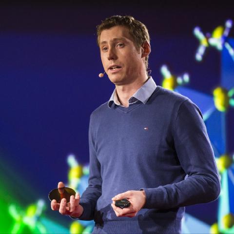
- Sam did a TED talk
- 1h 8m 13s
- Integrated photovoltaics
- 1h 8m 25s
- Group web page
- 1h 9m 27s
- Want to learn more about bandgaps? Check out pveducation.org
- 1h 9m 33s
- Scientific American wrote an article about The Perovskite Boom last year
- 1h 9m 54s
- Sam's lab is taking new students! Reach him via his web page or reach out to him on Twitter (@SamStranks)
- 1h 11m 59s
Transcript
Sam Stranks: This is The Amp Hour Podcast. Released March 10th, 2019. Episode 433. An interview with Sam Strengths.
Chris Gammell: Welcome to the Amp Hour. I'm Chris Gammell of Contextual Electronics. Hi, I'm Sam Strengths. I'm a physicist at Cambridge University and I lead a research group looking at new photovoltaic, new solar technologies and lighting technologies. Welcome, Sam. How are you doing?
Sam Stranks: Very good. How are you? I'm great. I'm ready to talk about some perovskites, which is a word that I didn't actually know until I think I watched your TED Talk about it. And then I reached out and you were very gracious to join us here. This seems like a new class of materials, but then I started reading back on Wikipedia and articles and stuff and it doesn't seem that new. So how new are we talking here?
Chris Gammell: Yeah, so perovskite is a huge family of materials. So there's a lot of naturally occurring perovskite minerals in the earth and they've been well characterized over the last 200 years. So actually the word perovskite is named after Russian mineralogist Perovsky and they discovered calcium titanate, which is the first perovskite.
Sam Stranks: Yeah, it looks like the shape is kind of part of it. Is that right? Like the shape is more than anything else?
Chris Gammell: Exactly. So it's the crystal structure. So it takes the crystal structure ABX3. And so in each of the ABX sites, you can have different atoms, different ions. And so calcium titanate is one where they have calcium, titanium and oxygen. But then there's a whole, so this is a naturally occurring class of materials, but then there's a whole lot of man-made perovskites, which are the ones we're working on. And in fact, they also have quite a bit of history. There's been sort of over the last two to three decades, in fact, even more than that, people have been working on these perovskites for different electronic applications. And particularly we have these, we're working on these hybrid perovskites, which have organic molecules in them as well. Yeah. And yeah, these were sort of, these were used for organic transistors in the 90s. There's a lot of research going on at IBM looking at these materials. And then, yeah, so they were used for transistors and they haven't really stepped forward much in that field.
Sam Stranks: One trick pony right now, but it sounds like they're definitely expanding.
Chris Gammell: Well, I think that's, yeah, that's the excitement that, so in 2009, then they got, they were first used in a solar cell. And that really, well, that was the very first used in a solar cell. And then 2012, there was a big efficiency jump. And that really started this wave of perovskite work. And in fact, ironically, this is now sort of reinvigorating this transistor community as well, as well as many other fields.
Sam Stranks: Oh, yeah.
Chris Gammell: Beyond just solar.
Sam Stranks: When there's like research papers around it, I'm sure that people are like, oh, I could try it for this and this and this. And then they start using it again.
Chris Gammell: And it snowballs and there's, you know, now there's, I mean, not just physicists, there's chemists, engineers, material scientists all working on it. So it's starting to invent new perovskites, new things we can do with them. So it's very exciting and a huge class of materials. That's great.
Sam Stranks: That's great. Yeah. And it's good to know too that it's like, it's more of the shape than it is the actual chemical composition. Because like looking at some of these chemical formulas, that ABX3, like you're talking about, like the A is sometimes really, really a long chain of something. And then the B is another chain of something. And it's, yeah, that's kind of crazy.
Chris Gammell: And it really completely changes the properties. So if you have a really long A, for example, an organic cation, you can make these layered structures. And they're very different than if you have a very small A site where you make these three-dimensional, very compact crystal structures. And they have very, very different properties, even though it's a very small change.
Sam Stranks: Okay. So before we jump into the technical stuff, what would you say the level of knowledge around chemical makeup and material properties people need to have in order to understand this?
Chris Gammell: Well, so I mean, from one level, not very much. I mean, I think that the elements we put in can be relatively simple, particularly for the solar technologies. Okay. But of course, you could go to a much higher and complex level, which we'll probably try not to go there today.
Sam Stranks: Yeah, no reduction oxidation, anything like that. No, no, we're trying to avoid. My chemistry class is haunting me from the past. Well, and I guess that would be a question for you then. How do you consider yourself? I mean, are you a material scientist? Are you a chemist? Are you an electronics person? What do you feel like you are?
Chris Gammell: Yeah. So I mean, my background is as a physicist. And I would say I'm mostly a physicist. But I do certainly don the hat of a chemist and of electrical engineer, of a chemical engineer, material scientists very frequently. And in fact, I could very well fit in any of those departments. And I think that's one of the exciting things that it really is this interdisciplinary work that is only enabled by engaging the chemists and the material scientists and the engineers together. Yeah.
Sam Stranks: I worked for a year and a half or a little bit more in a Samsung fab. And I went in and I'm like, oh, electronics. And then it's like, oh, no. Oh, this isn't electronics at all. I mean, you learn a lot. And it's great. But it's not resistors. Unless you're making the resistors of something.
Chris Gammell: That's true. Yeah. But I have learned a lot in this process as well. I mean, it is very exciting because you do learn a lot of different fields. And you have to learn very quickly.
Sam Stranks: Well, it seems like, I mean, you're on the edge of research as well. So that you kind of have to, you know, I read about the, you know, the transistor in the early days. You know, what's that book that I like? I have it up here in my loft somewhere. About the Bell Labs. The Idea Factory. I read that stuff. You know, about. Yep. Great book. But, like, you know, the stuff that they were doing, they obviously had big teams as well. But, like, they had chemical, you know, chemists. They had material scientists. They had mechanical engineers, electrical engineers, everyone. So you have to be really, really cross-platform. Exactly. How did you get to this point then? So you started in physics. But let's take a step back. Where did you get started?
Chris Gammell: Yeah. So, I mean, I was obviously raised in Australia. And I'm much sunnier climbs, at least here in Cambridge, UK. And so for my undergraduate, I generally, you know, like physics. I like science in general. Couldn't decide what I wanted to do. So I did a very general science undergraduate as a Bachelor of Science and actually a Bachelor of Arts. So I was covering sort of physics and chemistry as my majors for the science. And then applied maths and actually German studies for the arts side. Wow. So quite a broad undergrad background. And so, yeah. So, I mean, I enjoyed a lot of the work on particularly light and how light interacts with different materials. And so that naturally engages physics, but also chemistry of the different materials. And actually, my master's project, I actually, I wanted to do something joint physics and chemistry to bridge them both. And I ended up doing a very interesting project looking at protein aggregation in white wine. So one of the big problems for the wine industry is actually there's these proteins that aggregate and start to form wine haze in white wines. In fact, any white wine could have this problem. And so what the wine industry does is actually they use clay to filter out these proteins. Oh, really? Yeah. And they're still the state-of-the-art method today. So they lose a lot of wine. There's about 10% of wines lost through this process, through literally filtering it through clay. Because it just gets absorbed, basically? Yeah, exactly. Yeah. Wow.
Sam Stranks: So there's somewhere, there's like a rat in the bottom of a clay barrel just drunk off his ass, like, getting white wine. Yeah, exactly.
Chris Gammell: Wow. Yeah. So there's, you know, it's a $50 million plus problem for the wine industry. Yeah. And so one of the problems is that they don't actually know how this aggregation happens. And so my project was looking at how these proteins bind together, you know, so that if you know more about it, then you can start to target ways to prevent it from happening.
Sam Stranks: Yeah. Yeah.
Chris Gammell: And so that was very interesting as some, you know, modeling of how proteins stick together. And in fact, it's in some ways similar to aggregation in Alzheimer's and how proteins form these fibers.
Sam Stranks: Oh, like the plaque stuff? Exactly. Yeah. Yeah.
Chris Gammell: So they form these fibrils and it's a similar way in wine, although they're a bit more amorphous and a bit more blobby-like. But there are parallels there and some, you know, the modeling can in some ways help both. So that was a very interesting start. And it was actually very nice because I was working for the Australian Wine Research Institute and the University of Adelaide, which is where I did my undergrad. And they had a very nice policy because they were the testing center for wine for all wineries around Australia. So every winery would send in two bottles, one to test and one as a backup, just in case I had to test again. You see where I'm going with this? Yeah. So every two months, they would give the leftover wine out to the staff. So you get a case of 12 wine bottles, although half of them were usually very experimental, but the other half were very, very good.
Sam Stranks: Right. Right. Well, you know, you got to test them. You got to try them out. I'm sure you were very popular in the grad student population. Exactly. It was, yeah. Not a lot of extra dollars to go around for that. No, no.
Chris Gammell: But wine's a good currency.
Sam Stranks: That's right.
Chris Gammell: That's right. Yeah. So that's where I really engaged in this concept of trying to bridge physics and chemistry and trying to merge these worlds that typically are quite separate and like to keep themselves quite separate, I've found. Yeah. And then so that was 2007, 2008. And then I was awarded a Rhodes Scholarship to go to Oxford to do my PhD. That was the end of 2007. I was awarded that, which was very exciting and took me on a whole new adventure across the sea to the UK. Yeah. That's quite a distance, actually. Yes, exactly. Across the sea in many lands. And yeah. And so that was in 2008 when I arrived in Oxford and, you know, completely new place and a very, very different place and, but a very exciting place and lots happening. And so, you know, beyond just the academic work. But yeah, so there I started working on what's called carbon nanotubes, so really tiny cylinders of carbon. And yeah, the sort of, so there's the size of about a nanometer in diameter, so a billionth of a meter. Yeah. And the idea, what we were trying to do was wrap polymers around these nanotubes. And these polymers can harvest light and absorb light. And so, for example, sunlight. And then they could energize electrons and those electrons could inject into the nanotube and then zoom along these nanotubes to electrodes.
Sam Stranks: It feels like I've been seeing less about nanotubes these days. It seemed like it was very popular for a while. What kind of happened to all that stuff?
Chris Gammell: Well, yeah, no, it's an interesting one because, I mean, it's, so for carbon, you know, there's these fullerines, which are just basically balls of carbon. And they won the Nobel Prize. Are they like buckyballs? Buckyballs, exactly. And, you know, they won the Nobel Prize for that. And then graphene was, last, you know, in 2005, there was a Nobel Prize for graphene, which is the flat version of carbon. So nanotubes are sort of the odd one out. They're the, you know, they're very promising, very exciting. But yeah, they've, you know, they've sort of, I suppose, stagnated a little bit. And I think one of the big problems is that when you make nanotubes or just when they're made in the lab, you make both metallic and semiconductor nanotubes. And it's very, very difficult to separate them out.
Sam Stranks: We need a grad student with like really, really fine tweezers, right? Exactly. Yeah, exactly. And a very good microscope. Yeah, that's right.
Chris Gammell: And so that literally is-
Sam Stranks: A couple of bottles of wine to smooth the hands and everything, right? Yeah.
Chris Gammell: Yeah. And so that literally has, I think, been a big part of what's stopped them from being at least commercially used. I mean, they're very promising. They're very conductive. They've got some pretty amazing properties. So, for example, you've probably heard about this space elevator concept. Yes. Yeah. So nanotubes are a material that actually could be used for that. They're strong enough that they could hold. This is a tether going up to a satellite, for example, that you could transport things up from Earth. But they'll be strong enough that you could hold, that could hold its own weight, but it was not too heavy that it would collapse. But obviously, that's, you know, it's maybe a bit more science fiction or whatever happened. But also for transistors and other things, they could be very promising. But just because you've got this problem of you've got a whole lot of different types of tubes, it's very hard to sort them. And that's a big issue.
Sam Stranks: And it feels like it's that manufacturing piece, that technology transfer, which I'm sure we'll get into with the company you're involved with. But that is always, you know, like reading. I've learned to tamp down my enthusiasm when I'm reading my MIT technology review where I'm like, oh, my God, the future's here. And then it's like, oh, wait, no. That one still hasn't happened yet.
Chris Gammell: Yeah. I get friends all the time sending me articles they've read about the solar roads and all these things.
Sam Stranks: Oh, well, you know, that's a hot topic around here, too, but not in the positive sense.
Chris Gammell: Yeah, exactly. Yeah. And there's sort of, yeah, I mean, it's hard to sort of read between the gimmicky versus the realistic. And, yeah, although we should never dampen our excitement because there's always exciting things.
Sam Stranks: Well, I feel like I have to stand in for, you know, so Dave wasn't able to join us because, as you know, the time difference between, you know, Europe and the U.S. And Australia is splitting the world in three, so that's always tough. Yeah. But, yeah, Dave is a big fan of debunking. And I think he just talked about some graphene or some heater element that was based on nanotubes or something like that. Yeah. Yeah. Yeah. So, but, okay, so let's get back to the real, you know, the stuff that you're doing. I mean, so, like, so what made you transfer out of nanotube research into something else then?
Chris Gammell: Yeah. Yeah. So, yeah, so, so I finished my PhD in 2012 and then I was looking at next opportunities. My wife actually had another year of her PhD to go herself. And so I was looking at opportunities in Oxford and there was, so another group, so I did my PhD in a group, a carbon energy group, but another group, which is Henry Stathes' group, they worked on, so also in the physics department in Oxford, they worked on what's called disensitized solar cells. So these are, these are solar cells that basically have a dye that absorb light really well. And then they inject their charges into, into other materials that, that transport them and collect them electrodes.
Sam Stranks: Oh, it's like a collector, like a, like a, like a flower or something where it's sending it down the stem or something. Yeah, exactly.
Chris Gammell: It's just, it's just literally like a dye that absorbs and that's it. And then it creates electrons or energizes electrons, but then doesn't serve much for the purpose. So, so I, you know, I'd, I'd been in my background at that point was then new solar technologies in terms of the carbon nanotubes and various other things. And so I was keen to join Henry's group. And just so it happens at that, the time I joined as the summer of 2012, that it also had this, that just had this discovery of these perovskites in the lab. And this, this, this reemergence of the perovskites that, that came. So there was a graduate student in Henry's group who'd, who'd been to Japan on a, on a collaboration visit. And with the Japanese group, they actually developed these perovskites. And so they, I actually didn't know that they'd had this discovery in this paper. It was all sort of a little bit, you know, secretive because it was very new and, and, you know, exciting. And we didn't know what to, you know, what was going to come from it. And so when I joined the group within about two to three months, that whole group that was working on about 20 people, it was working on disensitized solar cells that pretty much transformed entirely to perovskite solar cells. The right turn. And it was just like, okay, yeah, we're doing this. Yeah. Absolutely amazing turn in very short space of time. Right.
Sam Stranks: Which, I mean, maybe you can give us a feeling for like, does, does that happen often in research groups?
Chris Gammell: No, not, not entire groups changing. You know, I mean, I mean, in the end it's still working on solar technologies, but it's just a completely different solar technology. Yeah. I mean, I, I really haven't heard of that happen at all from my experience. Yeah.
Sam Stranks: I mean, like my, my image of the academic world in the research realm is like, you know, you're, you're, you're in five year chunks of time. Like obviously you're doing a lot of stuff, you're publishing around a lot of different things, but it's these timelines because you're either on grants or you're, you know, you're, you're doing these longer, longer, or timeline kind of things.
Chris Gammell: Exactly. Yeah. And so, and so there's wider programs you're developing and yeah, so it's very rare for it to, yeah. And I mean, to be fair, it's very rare for such a discovery to come along as well that sort of, and that discovery that you can very quickly transition into. Right. Maybe we'll get onto that.
Sam Stranks: That curve, it sounds like if you're, if you're going up the curve that fast, it sounds pretty amazing as well.
Chris Gammell: Yeah. Yes. Yeah. And obviously people are excited to work on it as well because there is this, you know, very rapid progress.
Sam Stranks: Okay. So, so they, so you said 2009 was the first one. Was that the, in Japan? Yeah.
Chris Gammell: So that was, yeah. So Tom Miyazaka, a professor in Japan who, they, they made the first perovskite solar cell. And this was actually using, it was basically a dye-sensitized solar cell type system. So here the perovskite was the dye. So that it was absorbing light. It was a pigment basically that could absorb the light. And then these dye-sensitized cells are engineered so that they have these, these, these metal oxide scaffolds. So they're basically a scaffold that supports the perovskite. And that's also an electrode. So that, that metal oxide scaffold actually transports the electrons to an electrode where they're collected. And so, yeah, so they made the first one in 2009. It was, so the efficiency of, of the sunlight to electricity was about 3%. So not, not, not that, you know, not mind blowing and, and certainly not game changing at that point. And, and so it wasn't really, you know, no one really caught onto it, sort of overlooked really until 2012. And that was from the graduate student Henry States group who went to visit the group there to start working on them, on these things. And, and, and, and that kind of then reinvigorated it. Yeah. And, and one of the, it was, it was actually quite funny because one of the, one of the things that actually made it work was actually a mistake in the, in, in, in the amounts that were weighing out of the materials to make the solution.
Sam Stranks: That's how myths are built though.
Chris Gammell: You know, like that's how you have to have it happen, you know? Exactly. Exactly. It would, and, you know, I think you think back on it and wonder whether we would have completely overlooked this, you know, even till today if this hadn't happened.
Sam Stranks: Right. That's like the, the apple, the apple falling from the, you know, proverbial tree did it actually happen? Who knows? But in this case, maybe it's, you know, grabbing, grabbing the, the wrong size beaker or something, you know? Yeah. Yeah.
Chris Gammell: Well, it was, it was weighing, it was actually flipping around the ingredients and, and, and doing them in the wrong. So, so double one and half the other one. Yeah. And so, and then the solar cell just worked. It suddenly, so that 3% suddenly went up to 10%. And that's. Oh, wow. In the scheme of a solar cell, that is a huge breakthrough. And that's. Right, right, right, right. And these, you know, the dye-sensitized solar cells were typically three to 5%. And so, you know, in a lab that's, the record is 5% or around that sort of order when suddenly it goes 10%. Yeah, so to break the record out of the gate would be pretty, pretty impressive, huh? Yeah, exactly. So that, that was certainly a game changer. And then that, you know, that was summer of 2012 and all of that was, you know, there was a paper submitted and then the work was very quickly transforming into this, into, into working on perovskites. Mm-hmm. And so the other, I suppose, you know, why the big jump? So, so these, in, in Japan, in these dye-sensitized solar cells, they were using a liquid layer. So the, the layer on top is actually a liquid electrolyte and that's the other electrode. And that meant it was very unstable. So it would actually start to dissolve and degrade the, the perovskite material. Mm-hmm. And so one of the big jumps that took it up to 10% was that, was the graduate student replaced that liquid layer with a, with a solid state layer. So, so, so.
Sam Stranks: Of a similar, similar kind of makeup, but just it didn't have the same, the same mobility of ion. It wasn't liquid.
Chris Gammell: It was, yeah, it was just a solid layer of a film. And then that helped to, helped to jump it up to 10%.
Sam Stranks: Could you give us an idea of what the, the, what early days of research like that looks like? So like. Yeah. Are you doing like designs of experiment? Are you doing like, I mean, are you in, is it, does it look more like a chemistry lab? Does it look more like a semiconductor lab? Like what does it actually look like in there?
Chris Gammell: Yeah. So as in now or back then when we were doing this. I'd say back, back then would be good.
Sam Stranks: I mean, like, or you could give a general case too, because I'm sure it's going to transition.
Chris Gammell: So I think I would say mostly looking like a chemistry lab. And that most of these materials that we're producing, we, we solution process them. So they're typically, you know, we make their powders. We make them into solutions into, so we mix them up and dissolve them. And then we, we, we typically spin coat them down. So what we do is we take some of that solution. We put it on a, on a glass, a glass substrate. And we spin coat it at a few thousand RPM. And that makes a very nice uniform film. And so that's a lot of the, the processing kind of work is, is wet chemistry. So the, the typical lab, you know, you, we would see, you'd see fume hoods where students are working in. In fact, at that time it was all in a clean room as well. So they're, we're not only in, you know, we're in the bunny suits as well, uh, in the fume hoods. Um, and then also, so some of the work's done in nitrogen glove boxes. So here, this is, um, so I don't know if you've seen those, but you know, the gloves, um, which is sort of bordering more on the semiconductor fab type outlook. Um, but, but there it's in nitrogen so that it protects it from the environment, protects the samples from, from any oxygen or moisture. Um, and so, and so half the work's in that. So, so there's a chemistry aspect. There's, there's the semiconductor fab type aspect. And then we have, um, metal evaporators where we deposit down electrodes, um, which is again, more of the semiconductor side. Um, but then the testing is more of the physics side and that's where we have, so, so we test them under a solar simulator. So we have a big light source that reproduces or replicates the sun essentially. Um, it's, it's very much standardized of what, what we define as, as one sun. Um, so the spectrum and, and the intensity of the light is, is, you know, defined and fixed. Um, it's, I think it's, it's, it ends up being something like the average of, of the contiguous U.S. states of the, of the illumination intensity you see there.
Sam Stranks: Chicago's bringing that average down. Yeah, exactly. Yes. Yeah. Yeah. The South, the South helps out, I guess.
Chris Gammell: Yeah. Yeah. Yeah. Exactly. Yeah. Um, which is ironic because I always look at the sky in Cambridge and see, see cloud as well. So it's certainly not holding up.
Sam Stranks: I'm sure you have like some grad students that are like just slightly above average in terms of like, you know, vitamin D and, and, you know, lack of seasonal affective disorder just because they're working under those lamps.
Chris Gammell: Yeah. Yeah. Well, exactly. Yeah. This is the other thing. They're in dark labs. Yeah. All the time. Um, yeah. So, and then, and then, so the physics, yeah. So looking with solar simulators, but then we also do a lot of, and even back then, and also now in my lab, we do a lot of work, um, looking at, at lasers and how sort of putting pulse light onto these devices and seeing how they respond. Um, and I'm sure that's something we can, we can get onto. Um, yeah, definitely. Um, cause, cause that's sort of a nice way to look at, you know, when you energize electrons, how long they can live for, um, how many you can energize and, and, and how you, how well you can collect them at electrodes.
Sam Stranks: So like, so now we're kind of moving into the perovskite era, right? Yeah. And man, I hope it gets called the perovskite. That'd be cool. Exactly. It's a good, it'd be great. So could you, could you compare us against, uh, silicon or just, you know, generic photovoltaics these days? Like how do they differ, especially like in the processing and everything like that?
Chris Gammell: Yeah. So the, well, so, okay. So the solar cells, most people see on roofs, you know, the sort of the dark blue panels. Um, so they're crystalline silicon, um, is, is the, is the technology. Um, and so the, the main thing that differs is, is what the, I mean, what the absorber layer is. So in this case, this is silicon. Um, and, and usually it's, it's two types of silicon brought together to make a PN junction. Um, and, and then you have electrodes attached to them. So that the, you know, you, you, you illuminate them and then energize electrons and holes so that the whole was, you know, a lack of an electron, which we, we have to consider in this sort of situation. Um, and then the electrons and holes are collected at opposite electrodes. Um, and in many ways that a silicon cell is very similar to a perovskite cell. It's just that in the case of the perovskite, you have a different absorber there. The perovskite is the absorber. Um, but it's a similar style that you have electrodes then, um, to, to collect, um, these, the energized charges. Um, what, where it differs though, is that silicon is, is a very poor absorber of light. Um, so it's, it's got, it's got what's called an indirect band gap. So you need this multiple complicated processes to be able to absorb a photon, absorb some light and energize an electron. Um, so you have to make them very thick. So the typical solar cells are, um, something like, so a few hundred microns thick, um, which sounds very thin actually, to be fair, but it is in, in the sort of semiconductor, you know, scale. It's quite right. When you're in nanometers, when you're at nanometers, you know, then your orders of magnitude. Exactly. Right. Yeah. Yeah. Yeah. Um, so these are, you know, something like a fraction of a millimeter in thickness, um, and to be able to absorb enough light. And so, so the design of the cell is a bit different because then you have to manage how you get your electrons and holes out.
Sam Stranks: And I remember, I remember from like seeing like the super, super high end, like triple absorption, uh, photovoltaic cells that have been on like, like satellites. And that was meant for like different, wasn't it like they have different layers that have different absorption levels to get more light in there?
Chris Gammell: Is that right? Yeah. So these multi junctions then, so they have different, different absorbers, which harvest different regions of, of, of the solar spectrum. So some will harvest the red wavelengths, some will harvest the blue wavelengths. Um, and, and that you can essentially add together and get a much higher efficiency than if you just have one layer absorbing light. Yeah.
Sam Stranks: And what, what are the, what are the standard efficiencies these days? Like, so if you say you look at someone's roof, you're like, that's probably this much. You look at a, uh, a satellite is probably this much. Like what are those areas?
Chris Gammell: Yeah. So, okay. So, so the record silicon cell in the lab is, is it's about 27% efficiency. Um, that's on a small scale, relatively small scale cell. Um, when you connect those cells together and make a module, um, then that drops to about 20%. So the, the full module that you, so the panel you see on a roof is about typically at best about 20%. They're usually about 18 to 20% efficient, um, because there's losses in the scale up and the engineering of, of a full module. Um, so for, so yeah, so, so if we talk about just say the record lab cells, so 27%, um, so perovskite at the moment is, is it 23%? Um, and it's coming for it. It's coming for it. Exactly. I was at a conference last week and there was, there was an announcement of a 24% record now. So that's, it's actually jumped another 1%, uh, very recently, which is, which is actually quite staggering. Um, but, but then if we go to the, the multi-junction cells, so these, you know, very high, efficient, um, quite complicated stacks. Um, I, I believe once the record triple junction is about 39%, um, which is very impressive. It's, it's a very, very amazing, um, you know, semiconductor stack, um, because there are, you know, I'm not sure how many layers are on total, but there are many, many layers that are all optimized and just squeezing every bit of power out. It just sounds real expensive though. It is.
Sam Stranks: Those aren't, those aren't the ones that, you know, someone's putting on their house from solar city. No, exactly.
Chris Gammell: No. Um, and then this is the thing that, you know, you can get this high efficiency, which is great. And so for example, space applications cost is, you know, really doesn't matter. Um, right. Perfect. You want to. Reliability and everything else. Yeah. Reliability and producing a lot of power. That's, that's essential. Um, I mean, the silicon cells, even the complexities, I mean, it is quite complex. There are lots of different layers, um, particularly they, um, so for one thing to actually make the silicon pure enough, they have to bake it at very high temperatures, um, which, which does cost a lot of energy as well. So sort of typically 900 Celsius, um, they have to heat it up to, to bake out, um, defects and other blemishes.
Sam Stranks: On that topic too, if people haven't seen, there's YouTube videos of people doing it. So, uh, uh, Sam, who's been different, Sam has been on the show. He's, he's done, uh, uh, transitions at home. Um, Jerry Ellesworth, who has done, um, transistors at home, just showing that kind of stuff. There's diffusion furnaces. Those are the kinds of things you're talking about, right? Exactly. Yep.
Chris Gammell: Yep. Um, yeah. And then there's other layers as well of passivation layers and things that help to just tweak that efficiency up even further. Um, and then the multi-junctions obviously, you know, that complexity goes up again. Um, and I think, and that's really where the perovskite advantages come in. And that's, you know, they're very, very simple to process. Um, and in many ways, the solar cell we make, you know, we take an ink, one of these, these solutions that we've made and just cast it down. Um, you can also inkjet print it, for example, and make the absorb layer. And then we just sandwich them with, with two electrodes and you've got your solar cell. Um, so it's all very low temperature, you know, sort of 150 degrees Celsius maximum, which, which is very important from an industrial processing aspect.
Sam Stranks: A bunch of people in our audience just, just gasped as you said that. I mean, obviously it's very amazing, but also because I've been talking about printed electronics for a long time and there's been this ongoing debate. And so what's, I mean, so I guess we're talking about solar cells and that's, uh, you know, a simpler kind of thing. Uh, is this moving into transistor stuff at all, or is this kind of still pretty far off in semiconductor space?
Chris Gammell: Yeah. So, I mean, there is, there's a lot more work, especially in the last year coming out on, on transistors, uh, of these materials. Um, what I think one of the big issues, particularly for transistors is that, um, is that you have, uh, so, and one of the limitations of these materials is that there are irons that can move in them. And so when you want, you know, quite fast switching, for example, um, the, the response time might be limited by how fast the irons can move. Um, right. Or even whether you can have good kind of on-off behavior, whether you can actually make the irons move enough to ever have that. Um, that's where the challenges lie, but, but it's certainly, there has been some breakthroughs in the last, in the last year, at least. I mean, it, it probably is possible. Um, and, and that's really quite exciting, I think, because it does open up printable, you know, printable transistors, printable electronics, um, beyond just a solar.
Sam Stranks: And like large scale stuff to start with, it's not like you're going to do a seven nanometer transistor right away. No, no. Yeah. You know, doing like a transistor is kind of cool, you know, like a 2N3904. Why not? Yeah. Let's do it. Come on.
Chris Gammell: Yeah. And then, you know, if you, I mean, if you make them cheap enough as well, you can make, you know, many, many of them and put them out in the field anywhere and just think about, you know, all these internet of things type applications. Yeah. Yeah. Yeah. It's, it's, it's all possible, but there's still, there's a long road ahead for that at least.
Sam Stranks: Yeah, definitely. Well, and like you said, it's the, the focus is coming back onto it with, with the research now. So that's, that's an important starting place. Yeah. Now we're at perovskite. How does it work? Yeah. So we're back to this ABX3, is that right? Yep. Do I remember that right? That's right. That's exactly right. So how do you, how do you get started with this kind of thing? Like, so maybe what is the simplest version of a perovskite that you're making currently?
Chris Gammell: Yeah. So, so the simplest version we have, so, so the A is, is a very small organic molecule, such as, so methyl ammonium. So this is a, I see it's, it's got a nitrogen group and then a carbon group attached to it with a few hydrogens around. So it's quite small and, and that's the A site. B is typically lead, a lead iron and, and the X is halide. So iodide typically. So it's typically, so methyl ammonium lead iodide is, is our kind of the drosser filler of perovskites. Got it. Yeah. The standard system. And so that, that has, and that was, you know, the first one was used in a solar cell that absorbs light very, very strongly. So, you know, I was talking about silicon where you have, you know, 200 micro micrometers of, of material. Here you can bring it down to half a micron. So a few hundred nanometers of, of this film will absorb as much light as 200 microns of, of silicon.
Sam Stranks: Wow. Okay. That's, that's impressive then. What about the materials that are in there? Like, are those, are any of those super hard to get? Cause I remember like, is it like Indian phosphide? I remember they keep talking about putting more and more crazy chemicals that go into, aside from just the normal, you know, photovoltaic processing, but like to get efficiencies up there, like Indian phosphide, whatever, whatever, whatever, you know, like lots of weird things.
Chris Gammell: Yep. Yeah. So the, I mean, that, that is the, all that's in there. So it's, it's these, these three components that, that sit in a, in a crystal, uh, in, in these ABX3 crystal sites. And the, and the, and the thin film was just made up of, of those, um, all these little, um, unit cells linked together to make a film.
Sam Stranks: But are they hard, hard to get or make? Like, it's like lead kind of everywhere. I mean. Yeah.
Chris Gammell: So lead, no, they're, they're quite, quite rarely available. Um, the, the organic components, I mean, they're synthesized in lab, but the precursors for those are very easy to make. Um, lead and halides are, uh, are mined quite easily and, and quite abundant. So, so this is no, I mean, in terms of costs, uh, and, and shortages that there's, there's no issue there. Um, um, so the indium is a good example because at the moment we do actually use indium as the transport, one of the transparent electrodes. Um, and so indium obviously has some issues with, with, uh, with indium running out. Um, so we would have to be looking at potentially other, um, other elements than indium on the, on the electrode side, at least. Um, but for the actual active layer or the absorber layer, the perovskite, there's, there's no issue.
Sam Stranks: Okay. That's great. That's really great. Yeah. So what about, so, so you lay this, this level down and I guess, I guess I'm kind of having a hard time like visualizing it. Like, so you said you spin it onto like a substrate and this is like a, uh, a juice. It's like a juice that you spin onto a substrate. It spreads itself out. How do you then, so the, you're mentioning the electrodes, but how do you actually make that physical connection? Cause it feels like without having like a little tiny soldering iron, I don't really understand how it would actually collect these electrons like you're talking that makes. Yeah. Yeah.
Chris Gammell: Yeah. So, so maybe I'll talk you through the stack actually, cause then it might make more sense. Um, so on the glass, so we take a glass. Um, so, so in the, in the lab, we usually use something that's sort of half an inch by half an inch, a little small glass wafer. Um, and then on it, we have some, um, some transparent oxide. So indium tin oxide, for example. Um, and that's our bottom electrode. So that, that's across most of the glass.
Chris Gammell: In fact, it's, we usually pattern it. So it's not completely over the glass. It's not, you know, we can just measure a smaller area, for example. Um, and then we put our perovskite layer on top of that. Um, sometimes with a, with, with another metal oxide in between. Um, and then that, that means that, um, there's a direct, they see, uh, um, a planar, um, junction between them. Um, so there's just a flat layer between them and that, that is the electrode. So that, um, when we energize electrons in there, then the electrons will travel down to that bottom interface and then they get collected directly.
Sam Stranks: Doesn't something need to close the circuit? Like am I missing something? Yep. Okay.
Chris Gammell: I am. Okay. Okay. Um, so, so then we have a top layer on top, which is the other electrode. Um, so here we have, um, so it's often an organic. Layer, which is, uh, which is a collector of, for example, the holes. And that's, so, so we're basically making a sandwich stack. So we have just a layer on the bottom and the perovskite and then a layer on top. Um, and then we evaporate our metal electrodes, a metal, metal on top, which is what we can actually contact to measure it. So then we, so, and usually they're patterned. So we have fingers of those, for example. Um, and then we can come in and, and contact one of those. And then, um, we make a contact with the, with the bottom electrode with the other pin. And then that, that then completes the circuit.
Sam Stranks: So does the top layer inter, just interfere with the sunlight though? Or like what is, I'm visualizing like, like almost like a capacitor in this case where the, the dielectric in this case is actually the perovskite. But then I think of a, you know, like a parallel plate capacitor. In that case, the sunlight gets in the middle or it gets in the way of the top plate gets in the way of the light. So what's, what's, is it passing through something?
Chris Gammell: Yeah. So there's, I mean, there's different ways to do it, but most of the way we do it is actually we illuminate through the glass. And so, um, so, so through the glass we have, so that bottom layer, that indium tin oxide, for example, that's transparent. So then the perovskite, we illuminate through the glass, which is transparent. And then that can directly excite the perovskite. Okay. So there's nothing blocking it in the way, but then on top, obviously then there's, that's opaque to the light, but it doesn't matter because everything's absorbed below it. Right. Um, there are other designs where you can have, where you can illuminate from the top. If you have very thin fingers, for example, but that's, they're a bit more complicated and, and, and more lossy.
Sam Stranks: I didn't realize that indium tin oxide is, is transparent. Why, why is that?
Chris Gammell: Um, so, so it has a very large band gap. So it's something that, um, it absorbs somewhere in the ultraviolet region. So it means any light coming in that's, um, lower energy or, or longer wavelength, then then, then the, then the ultraviolet is, is transparent. It passes straight through.
Sam Stranks: Huh. Okay.
Chris Gammell: Um, you, you can change the indium tin oxide depending on the doping of it. You can, you can put other things in it and change the ratios of each of the elements to make it more absorbing if you so chose. But the, the type we use, the particular type is transparent.
Sam Stranks: Does that mean like what, what is the spectrum that the actual perovskite, um, absorbs in? It obviously doesn't, it doesn't get any of the UV light because of the, the indium tin oxide.
Chris Gammell: Yeah. Okay. So yeah, there's some loss from that, although it's, it's, um, at least for the, for what we want to harvest, there's not a lot of power in that, in that part, in the, in the deeper UV anyway, um, that we would lose. Um, so the, the perovskite absorb in principle can absorb everything from, um, sort of 250 to 300 nanometers up to, um, about 800 nanometers. So it's really quite a, almost all the way across the visible spectrum. So right from the real, the blue UV at 300 nanometers, right to the, almost to the near infrared at 800 nanometers.
Sam Stranks: That's great. And, and, and does that compare differently than, uh, photovoltaic is like certain regions that are different?
Chris Gammell: Uh, so, so silicon that she can absorb right across. In fact, it absorbs even to a little bit longer wavelengths. So it actually can absorb a little bit further into the near infrared. Um, um, so, so when I say it can absorb to 800 nanometers, that's the typical perovskite we use. So this methyl ammonium lead iodide, um, but we're, we're also looking at trying to tune that to get the absorption, you know, to be able to absorb further into the near infrared as well, like silicon.
Sam Stranks: And, and what is the benefit of that?
Chris Gammell: Is this that you absorb more of the heat stuff? Um, no, you can just, I mean, all of that light that you're absorbing still can be converted into electrical power. So that's still got it. Got it. Yeah. Even out to sort of, so a thousand nanometers, we can still in principle convert that into electrical power. And we, and we ideally want to as well.
Sam Stranks: Yeah. I guess that ups your efficiency in general, huh?
Chris Gammell: Yep, exactly. Yep. The reason it's not, you know, not very high, sort of even 27% of the limit is, is what silicon is at. Um, the limit is about 32% for just one layer of material. And that's just because you can't absorb. Um, you just can't absorb. You have to have some band gap, um, and you can't absorb photons that are lower energy than that band gap. Um, got it. And so there's a compromise in that you, um, you want to absorb as high energy as possible to have a high voltage, but then have a low band gap to have a high current. Um, and so it turns out 30, 32% is about the limit.
Sam Stranks: And that's like the maximum PowerPoint tracking kind of thing where you're balancing current and voltage. That too, yeah.
Chris Gammell: So, so, or this is just, if you had a perfectly, you know, uh, perfect conditions, um, where it was perfectly tracking the sun, um, you are limited to about 32%, even everything being ideal. Um, practically we probably never gets that probably about 30% is about what we'd actually get to. Um, but that's when multi junctions come in because that limit then goes up to about 50%. If you can, uh, if you have two junctions, for example, what's called a tandem solosol.
Sam Stranks: And so does that mean that perovskite has that same limitation? Yes.
Chris Gammell: Of the band gap stuff? So if we just had one layer of perovskite, it would, it would also only be able to get up to about 32%. Um, but then we couldn't, we can move to, to tandems with perovskite having two layers, for example, or three layers even of, of perovskite and really push beyond those, those limits.
Sam Stranks: Right. And I guess if you're processing simpler and you can get the light through transparent layers and everything, then you could start to have, you could have layer on layer and just, it'd be simpler to, to, to stack things up. Yeah, exactly. Yep. Well, you had mentioned the, uh, the lasers, uh, kind of targeting your, like testing. Could you explain that setup and why you do that?
Chris Gammell: So what we do, we have, we have lasers that, that produce, that have pulses of light. Um, and so these are very fast pulses. So usually something like, um, a picosecond, um, so a thousand billionth of a second, um, or even sometimes even faster than that. Um, and what it does is we, we, we shine them on our samples and we, we, we create a pulse of light, which then creates a pulse of energized electrons. Um, and then we monitor how those electrons then, um, lose their energy. So whether they, um, recombine with, uh, with each other, um, or they recombine with, uh, or they, or they reach traps. So they hit defects, um, and lose their energy or whether they are collected at the electrode. And we can monitor all of those things. Um, and so we can, we can get an idea for lifetime of these energized charges. And, and that's very important because we want to know, we want to obviously maximize how many electrons can be collected. Um, and we want to minimize how many of them are lost traps. Um, so it's a very, using these lasers is a very good way to, to, to measure this and to look at this. And then, and then we can go back and look at our material and try and optimize it, uh, to try and get rid of some of these defects, for example, and then see if we can improve this lifetime and prove how long they're energized for. What, what causes an actual defect? Yeah. So there's, there's, there's lots, lots of different types of defects, but the common one is, is a missing iron. So there's ABX three, it might have one, one site might be missing an X. Um, and so that creates what's called a vacancy and, um, and an electron could fall into that, um, that trap and then, and then lose its energy to heat.
Sam Stranks: So does that mean that the, the, because the X is doing the actual transport of electrons between these different sites, I guess maybe that makes us dig into the structure a little bit more.
Chris Gammell: Well, it's not really actually. So the, the full ABX three is involved in the transport. Um, it's just any of those sites that are missing create sort of a dip in the energy, um, energy landscape, which, which an electron could fall into like a well, sort of like an energetic well. Um, and it can't get out typically. Um, but one of the, I think most fascinating things about these perovskites is that they have quite high defect levels. So for a semiconductor, actually there, there are quite a few defects there. Um, so something like, um, one in a million of these, of these unit cells of these crystal sites have a defect. Um, that doesn't sound like much, but it's, but it's actually quite a lot.
Sam Stranks: Yeah, it adds up. It adds up. Yeah.
Chris Gammell: So these electrons, um, you know, it really shouldn't be working, but for some reason they are working. And it seems there's this, some sort of defect tolerance in these materials that we, we don't fully understand yet. Um, and it's really quite an exciting thing actually that, um, you know, we're taught in our semiconductor textbooks that, that we need to have a perfect crystal site, crystal lattice have no blemishes, no defects. Um, and, and this is kind of making us rewrite that textbook a little bit because they are working even in spite of quite a few defects. Well, but you're not using silicon in this case either. Right. That's true. That's true. And yeah. And for comparison, so silicon has, um, about a million times fewer defects than, than a typical perovskite cell. Yeah. Um, and if you had the same level of defects as you had in perovskites, um, in the silicon, you would, you would have no operation at all. You would have all traps. I see all the electrons would be trapped.
Sam Stranks: Yeah. Well, it makes good for a good manufacturing stuff.
Chris Gammell: Yes. Yeah. Yeah. So it seems to be tolerant to, you know, and that's why it's tolerant to making them quite easily and quite cheaply, um, because they are tolerant to these defects.
Sam Stranks: Could you explain the, uh, so, so you'd mentioned the, the entire ABX3 helps with the structure. What about it actually makes that electrons are mobile between, between this sheet of stuff that you're laying down?
Chris Gammell: Yeah. Um, so, so most of the, what's called the band structure. So what the electrons see, so there's, we have conduction band and valence band. Um, that's, that's made up of, of the, primarily from the bonds between, um, the B and the X. So usually the lead and the iodide. Um, so that dictates how, you know, what the energy levels are of these conduction bands and valence bands. And they're the, that's the region that the electron moves through. Um, so essentially they, all of these unit cells connect together to make, um, an energetic landscape that the electrons can move along. Um, and that's primarily the dictated by this lead halide bonding network.
Sam Stranks: Okay.
Chris Gammell: Um, so, so in many ways they do move along these, um, lead and iodide sites. Um, but it's, but it's quite smooth movement.
Sam Stranks: What, what, what is the air of the A there for then? Like, I guess.
Chris Gammell: It's a good question. But I mean, the, the, the, the A mainly, um, cause these lead and iodides are in, they're in octahedra actually. They're, the, the bonding makes them form octahedra. Um, and the A's sit at the corners of these octahedra and they, and they, they kind of compress the octahedra a little bit or, or expand the octahedra a little bit. So they influence them still. And, and this is one of the interesting things because you can then start thinking about other A sites where you can change how that octahedra is, is stressed. Um, and you get very different properties. Um, so the A is still quite important in, in dictating how the lead and iodide bond.
Sam Stranks: Oh, sorry. I was like bond to what? Bond to each other. Sorry. I was like, bond. Yeah. I was like, oh, so how much they bond? And I thought, I thought we cut out there. Yeah. No, no. Okay. Yeah. Yeah. Yeah. Of course. I mean, they have to bond do each other. Yeah. Bond is a verb. I know that now. Yeah. Yeah. I'm, I'm, I'm looking at the, uh, the, the, I mean, I'm, I'm, you know, I, I lean very heavily on Wikipedia in general. No, it's a good resource. And the octahedra shape you're talking about, it, it seems like there's a large size difference as well. Is, is that, is that realistic? Yeah.
Chris Gammell: So the, the lead is typically quite large and then the iodide is much smaller. So the lead sits at the center of the octahedron and then the, the iodides are decorated around in an octahedron around that lead. And so a lot of the properties of the materials we're working in are sort of unique to that octahedron. Yeah. And then how it's influenced by the A site.
Sam Stranks: Um, I guess the other thing I think back to about my, my semiconductor classes is like thinking about silicon having like the, the four donated and the four, you know, like the, the, the four spots where it all bonds together. And like that, if I'm thinking about that, right, I guess that's carbon as well. But, but like, it was very, uh, the math seemed to work out pretty well in my mind. Yep. And so lead is, is this really heavy, really large molecule. Like what, what about it makes it so that there's that, is it eight sites total or like how many bonding sites are there?
Chris Gammell: So, so, so you hear the difference between, so those, those other ones are covalently bonded. So they're directly bonded, um, materials. Um, so here they're ionic bonds. So they're, they're ions that sit in sites and there's an energetically favorable situation where they sit, happen to sit in octahedra. Um, and the charge is still balanced though, because, um, the unit cell, which is the most fundamental unit of this, um, is still charge neutral. It still adds up to be charged neutral. Um, it just so happens that they end up stacking in, uh, in octahedra. Um, and I think that's the, the interesting thing about ionic systems is that they're somewhat softer and they can have different types of rearrangements, different types of arrangements that can still be energetically favorable. Um, and partly why these materials have such versatility as well, because they are ionic and, and you have, you can make them move and you can make them, you can substitute certain ions for different ones without changing the structure too much.
Sam Stranks: Right. It seems like, uh, with silicon, it's like, it's so fundamental and low level and like so few things happening there. Maybe that drives that purity we were talking about as well, because if you don't have it, you, you can't really operate. But it seems like this is a more complex structure in general.
Chris Gammell: It is. Yeah. Yep. Um, yeah, there's, there's, there's a lot, a lot happening there. Um, and there's, um, at least there are some interesting thing, you know, thoughts that it is something unique about these lead halide systems, um, that you can have, um, this defect tolerance is, is actually associated with this specifically with the lead and halides. Um, and so for example, uh, when an electron moves along the perovskite. Um, and so there's, there's this idea that there's sort of the electron has almost like a force field around it, um, which, which blocks it from recombining with, with traps or with, from other charges. Um, it's, it's, it's what's called a polar on where the charge itself actually disturbs the other atoms around it and the other ions around it. Oh, really? Yeah. So there's some very interesting physics there that sort of, you know, on a, you know, not completely well known yet, but certainly some interesting, uh, fundamental science there still to be done to try and understand that.
Sam Stranks: Yeah. You know, that's another thing that like strikes me about like the early days of silicon processing. I was watching this Japanese documentary around the transistor and obviously they were, they were recovering from the war. Um, and so like, it seemed like they didn't have as much equipment, but probably still, you know, you know, similar to what was happening at Bell Labs and stuff. And it's just like, oh yeah, they didn't know what was going on at that point because it was still so early. And, and it seems like we're kind of in that era now with, with this kind of thing, with this, this structure. Yeah.
Chris Gammell: And I think, I mean, yeah, one of the interesting things is it's, it's just kept working. So just empirically, the devices keep getting better and better. And our fundamental understanding is still slightly lagging behind, uh, the actual, you know, right. The efficiency is out. It's sort of, it's quite a unique system in that sense. Usually most photovoltaic technologies that have developed over, you know, many years, for example, silicon, we knew a lot about them and therefore we, we could make them a bit better because we knew everything about them and knew what was limiting them. Whereas these, you know, empirically they've just kept working. Um, and, and I know at some point we will properly catch up on the fundamental science of it. Um, but, but, you know, until then we haven't yet hit the plateau. That's good.
Sam Stranks: I mean, progress is driven from the, just keep reaching and hopefully get more efficiency.
Chris Gammell: You know, as a physicist, I hope, I hope we do get the understanding and then start really driving it up even, even more, but that's, you know, it is still exciting to see it keep getting better in the meantime.
Sam Stranks: Yeah. Well, and let's talk about, uh, you know, some of the unknowns here. I mean, like I look at, I look at your, um, your research site on the, on your Cambridge research site and it's like listing all these applications, like, oh my God, you guys are going to use this for a lot of different things. Yep. So what are some of the, the non-solar applications that, that are also being targeted?
Chris Gammell: Yeah. So the, probably the, the, the, the main, or at least our first, uh, the one we're looking at the most is, is light emission. Um, and so here, um, in, in, in the simplest way, it's an LED, for example, is just a solar cell run in reverse. So in this situation, we're actually, um, injecting electrical charges in and then making them recombine and then emit, emit photons that emit light. Um, and so these, these perovskites are, uh, I talked about how they're good, very good at absorbing light, but they're also very good at emitting light. They're very efficient emitters. Really? Um, which, which is really quite exciting because we can have, um, you know, quite cheap, cheaply processed LEDs, um, and have very, very good color purity. Um, these, the emission, um, the, the, the widths of the emission spectra are actually really quite narrow. Um, and so this is pretty, this is very exciting for, for display applications. So you can think about having, you know, very crisp blue, red, and green emitters, um, in a similar way to the OLEDs, um, or quantum dot LEDs, um, are starting to, you know, starting to show.
Sam Stranks: Yeah. That's, that's amazing. And it's all, I mean, it's all based on band gap, right? I mean, that's, so that's kind of like what it all kind of comes back to is the, it hops down this band gap, it emits at a certain frequency and same thing with absorption, right? It's absorbing at certain frequencies better than that kind of thing. Yep, exactly.
Chris Gammell: And they're entirely reciprocal. This, you know, absorption and emission, they're, yeah, fundamentally based on the band gap.
Sam Stranks: Right. As anyone who knows who has, has an LED circuit and then there, the light goes on and they're like, wait, why is there all this noise in my circuit now? Exactly. It's the fluorescent lights when they're on, I see all this noise, what's happening? Oh my God.
Chris Gammell: Exactly. Yeah, it's fine. Yeah. And so we actually, and quite ironically, we actually look at for, even for solar cells, we look at the light emission of these materials because it tells you a lot about whether the solar cell is actually, you know, is, is operating well. It's a little bit counterintuitive that we want to make the solar cell emissive and emit light, but it actually tells you a lot, a lot about defects because if, because if you have your charges in your solar cell, they can either recombine and emit light or they can hit a trap and then lose energy to heat. So light, light is actually a very good probe for, for power losses in the solar cell even. And so a lot of these, the laser techniques I was talking about, when we excite them with a packet of, of, of energy of, then we look at actually at the light coming out then. That's a very good, nice way to look at whether a region is full of defects or has fewer defects. That's really cool.
Sam Stranks: So did I, did I read you guys are also using this for, for laser generation as well?
Chris Gammell: That's the other, yeah. So, I mean, the, the, so, so they seem to be good for lasing materials as well. Um, and one of the, one of the overall goals is, is to make an electrically pumped laser. Um, so typically we can, we can excite them with light and they can laze. Um, but the, the Holy Grail is actually making it so we can electrically inject the charges in, um, like an LED, but, but then get lasing output. Um, and, and that's quite a challenge, but it seems that these materials could be promising for that. Um, in that we can have very nice, um, nice emission spectra, which is essential for lasing. Um, and also very few defects as well.
Sam Stranks: Would that make it, uh, for like doing like optoelectronics and stuff like that? Would that be the, the eventual goal?
Chris Gammell: Yeah. So you could, you could envisage, you know, perovskites being used in many, many different things. So you've got the solar cell, but then also an LED, I mean, transistor, a laser, all these different units of optoelectronic units could in principle be from a very similar material family and produced very cheaply as well.
Sam Stranks: So what about the, so you had mentioned in Trent and perovskite based transistors, they have trouble because of turning on and off and transferring electrons through them. Does that not apply for like a lasing application?
Chris Gammell: Uh, it will as well. And, and that in particular, if you need fast, you know, some sort of fast lasing application. Um, and, and it all, it all comes back to this iron motion, um, that could be an issue for some of these other applications in particular, um, even for solar cells as well, actually, that while you're operating, um, and injecting charges, for example, you can have ions that actually move over time. Um, and this could lead to some quite serious stability issues. Um, and it's, that's one of the big challenges actually in general in, in these perovskites is to, to try and mitigate that iron motion and try and freeze it out if we can.
Sam Stranks: And that, that's just going to be again, like, like studying the chemistry and studying change.
Chris Gammell: Exactly. Exactly. And we've found actually some, some quite good, I mean, even over the last one to two years, there's been nice breakthroughs there where, where this, I talked about this A-site, this, this methyl ammonium, very small molecule we put in. Um, we've actually been swapping that out for slightly different molecules that slightly larger that can actually stabilize the iron migration, um, and iron motion a little bit at least. So there are hints that there are ways to do it. Um, we're not there completely yet, but I'm very encouraged by that, that we can do it. Yeah. Um, and, and that's where the chemists will really come in, will come into their own.
Sam Stranks: Well, and so you mentioned the past one to two years, it sounds like you're also, uh, cranking out some new things with Swift Solar. So tell us about Swift Solar.
Chris Gammell: Yeah. So, so I've, um, a co-founder of Swift Solar and there's, um, so there's the five other founders. Um, and, um, and so, and so, well, the history behind that was a few of us were previously working together in, in Henry State's group in Oxford. Um, I spent some time at MIT, um, and, and met one of the other founders there. Um, and a couple of the other guys went to Stanford as well. And so, you know, we're, we're quite passionate about this.
Sam Stranks: So not a very well-educated bunch. It sounds like, it sounds like you guys are here. Right. Not many, not many degrees in the room. No. Um, yeah.
Chris Gammell: So, so we've, we've been, yeah. So over the last two to three years been, um, sort of developing these ideas. Um, and what we're particularly looking at doing is, is, is making these, um, these tandem cells. So this is where we combine two proff scut layers together, um, to, to really go to high efficiency. But, but what we're also doing is making it, making lightweight, um, versions of these cells. So here, instead of putting them on glass, for example, we can start thinking about putting them on, on plastics or on, um, on metal foils that, that are very lightweight. And so this has some real advantages in, in terms of, um, installation, for example. So you could, you could, you could think about a role, a role of very high performance solar sheet, like a tarp that you can roll out on your roof and, and, and, you know, very easily and cheaply install a panel. Um, uh, you know, one idea would be, you know, sometime in future, you go to home depot and depot and, and, and, you know, just cut off a solar sheet and take it home and roll it out.
Sam Stranks: Yeah.
Chris Gammell: That would be there. That'd be great. The ultimate goal, but you know, there's a lot of challenges there, but, but it really the, the opportunity is, um, is, is, I mean, solar at the moment is, is essentially limited by cost. Um, and one of the ways to bring down costs of not just the actual panel itself, but also all the other things like installation and wiring, um, is to go to high efficiency. So really the drive is to go, you know, beyond this 32% limit to, to these tandem structures that can push us well into the 30s, 30% region. Right. Um, yeah.
Sam Stranks: Yeah. I, uh, I have a guilty pleasure of watching a tiny home videos and, uh, it's embarrassing, but, uh, I do. And they only fit like four solar cells on their roof and it's usually about like 1200 watts, I think max. And so you're saying like, you can maybe make that two and a half kilowatts or, you know,
Chris Gammell: more. Yeah. Well, that's kind of like the idea. Yeah. The idea, I mean, if, if we think about, uh, you know, let's say today if, um, the panels are 20% efficient, um, we want to at least take that to, to 25%. Um, and it doesn't sound like a lot, but it is, you know, so it's 20% more power roughly. Um, yeah. Yeah. But it, you know, it does make a huge difference, especially in the economics of solar, um, plus
Sam Stranks: the scale of the payback periods and stuff like that.
Chris Gammell: Yeah, exactly. They, they come down, but also the scalability as well. Cause one of the limitations of silicon is actually trying to make enough panels. You know, if we wanted to roll out enough silicon panels to power the world, um, at best it would take 40 to 50 years of just continually producing panels to get there. Whereas with perovskite, you could, you could do that in three to four years in principle. Um, so there is actually, uh, you know, this, this scalability issue as well that, that silicon might not get us all the way there if we did want to take renewables or at least solar all the way up to very high levels, um, of deployment.
Sam Stranks: Well, is there any downside? So like, uh, so assuming that it was like printable on a, like a thin plastic sheet kind of thing, is there a downside to just printing at 20% and going with that? Like, I don't, I don't understand the, I get some of the economic questions, but like, why hasn't this started and the production? Yeah.
Chris Gammell: Well, I think one of the issues is that's, I mean, well, one of the great things is that silicon is, is, is very good and it's coming down in price very, very quickly. I mean, that's great. Um, and so what, what's actually will happen. And in fact, it's already happening is that the cost of the actual module itself, that the material on the panel will be almost nothing. It'll come down to something like 20 cents a watt. Um, oh wow. Okay. Um, but in, but then there's the other thing. So there's these balance of systems costs. So there's the installation, the wiring, the inverter. Um, these are all starting to now dominate the costs of a solar installation. Um, so there's sort of something like, you know, a dollar a watt or something like that. And that's harder to bring those costs down. Um, so essentially the, you know, silicon costs nothing to make, even if peroxcat costs nothing to make, it couldn't compete unless it can either be cheaper on, you know, some of the other aspects or higher efficiency. Um, and so, oh, okay.
Sam Stranks: Yeah.
Chris Gammell: And so higher efficiency.
Sam Stranks: So you're saying because of, because you don't need to have as much other overhead type stuff like the framing and the, the wiring. Yeah.
Chris Gammell: And that's so with the lightweight aspects, um, that, that particularly brings down. So the cost of installation comes down a lot because we can, you know, you could have one person installing on a roof, rolling it out rather than having this complicated racking system that you have to put on your roof. Um, and the, and the other thing is efficiency. So we could, we can go beyond silicon with these tandems. And so if we increase efficiency, that also brings down the cost of, you know, the entire installation because the cost per watt then comes down because you're producing more power for that same amount of infrastructure.
Sam Stranks: That's really exciting in general. I mean, like the idea of like, I think I'd seen, maybe it was in your Ted talk, which will obviously we'll link it as well. Um, but, uh, someone was talking about like the, because it's, you know, quasi transparent as well, maybe even like putting it onto like windows, that kind of idea. Yeah.
Chris Gammell: And that is, yeah. And that's, that's a real possibility with, you know, the building integrated photovoltaics type model where you can think about, you know, designing it into the building. Um, I think the, I mean, at least the, um, you know, the opportunity to produce very large amounts of power is reduced with those. That's the sort of more smaller scale installations. Um, the, the rooftop and utility scale solar is sort of where the real opportunity is to, to really make a difference in, in terms of climate change, in terms of renewal. Um, powering things, but there are opportunities to do that. And then I'm sure we'll start to see, um, uh, commercialization of the, from the building integrated side as well.
Sam Stranks: That's great. That's yeah. That's really exciting. Well, um, this is, I mean, amazing that this stuff is, I think personally, like I, I think about like the fact that people just go and make an, you know, mix some chemicals together and like, Oh yeah, we got a new way to harvest energy. That's like kind of the dream. That's like Tony Stark type stuff. That's amazing. Um, so I appreciate you coming and talking to us about this. Where can people find out more about you and your research and, and maybe even some background info in case they don't understand photovoltaics and.
Chris Gammell: Yeah. So, so, um, well, there's, I mean, there's a few resources. I mean, obviously you can check out my own group webpage, but that may be more on the, on the technical side. Um, there's, um, well, there's, there's a, there's a quite a nice website. So pveducation.org, um, is, is quite a good, uh, quite a good resource for finding out about just, just photovoltaic technology in general. And they have some quite nice animations and things to explain a bit more on that. Um, I think in terms of perovskites, there's, um, there's, we had a scientific American article a few years ago now, um, on the opportunity, particularly around these tandems. Um, that, that could be quite a good resource for those wanting to find out more. Um, and, uh, I mean, I think, you know, there's, there's quite a bit of, quite a few articles coming out, um, on perovskites and their potential. Um, you know, so there's, you know, generally.
Sam Stranks: A little joke there with the potential. Yeah, exactly. Yeah.
Chris Gammell: Um, yeah. And I suppose, I mean, you know, I suppose just to make sure it's not just hype. I mean, you know, there are still some challenges that we do need to solve from the, from the lab side and from the, from the scale up side. Um, and, and one of them is, is, you know, we have to make them last on the roof for many years. That's, that's a challenge we need to make sure we can, um, we can validate. Um, and, and so we, you know, we and many others can perform stability tests where you do accelerated lifetime testing. For example, you simulate them being out in the field, putting them, stressing them under similar conditions. Um, but that takes time and, you know, to really validate them and for someone to underwrite a panel for 20 years, you really need some very strong and convincing data behind that. Um, yeah, definitely, you know, I always say it's quite, it's funny that, you know, in solar, they have a product that they'll guarantee to last for 30 years, which is just amazing, you know, to have an electronic product that can be guaranteed to be operating for that long. Um, yeah, it's fantastic. So the bar is set and that, and that's something that does need to be, you know, we do need to get there. Um, and I think that there is some encouraging stability data now coming out, but it's something that will take time. And that's why, at least why, you know, we're not seeing it on the, on the shelves today. Um, but I think in the next two to three years, we will start to see the first products and the next five years really start to see, you know, quite a lot of infiltration of, of, of some serious perovskite panels.
Sam Stranks: Awesome. Are you guys, uh, are you taking new students at your, at your lab or is that something people should even reach out? Yeah.
Chris Gammell: So please do reach out if you're interested in, in, uh, you know, in, in a PhD or, or masters, um, uh, or, or postdocs looking at, at these perovskite materials, please do reach out. Um, and, uh, likewise, Swift Solar, if you're interested in hearing more about it, we have some, uh, contact there on our website. You can check out Swift Solar, um, and, and, and follow us there. Um, yeah, absolutely. We'd love to chat with people interested in, in learning more and, uh, and working with them.
Sam Stranks: Great. And, uh, I saw you're on Twitter as well. So we'll, we'll link that, uh, we'll link that too. Is that, that's usually how we, we communicate here at the Empire. Please do. All right. Well, Sam, thanks so much for telling us about this. I appreciate it. Thanks, Chris. Thanks for having me on. It's great to chat.
Archived Discussion (2)
Comments are closed. Archived from the original site.
Show archived discussion (2)Hide discussion
ABX3CambridgeCarbon NanotubesCellEfficiencyGrapheneIndiumlaserLEDOrganicPerovskitesPhDSemiconductorsolar
Keep current
Every episode, plus the occasional job post, in your inbox.
1. Their stability is much worse than your standard silicon based solar cell, even if you make a super good seal to keep moisture out from what I recall they still degrade after a month or two (20% drops to 15% and so on)
2. They have really interesting IV curve behavior in that if you scan from 0V -> OC voltage when characterizing them you will get a lower peak efficiency than if you were to scan from OC -> 0V. I don't think anyone has given a full answer as to why but it seems to do with the formation of temporary dipoles when doing a reverse scan. Anyway, what this means is when someone says they have a perovskite solar cell that is 25% efficient you need to ask how they did the IV scan, because you might find that its 20% in one direction and 25% in other
Also big thanks for Chris & Sam on this episode, was really interesting to hear how the progress of perovskites is going since I last looked at them a few years ago