
#390 – An Interview with Sam Zeloof
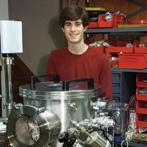
Download episode · 89 MB
Also on Apple · Spotify · YouTube · RSS
Show Notes
- Welcome Sam Zeloof!
- Sam is graduating high school soon, he's currently finishing up his senior year.
- Sam started the process of making semiconductors in his garage 1.5 years ago
- 0h 1m 15s
- Sam was inspired by Jeri Ellsworth's videos
- 0h 2m 45s
- He'll be attending Carnegie Mellon University in the fall.
- 0h 8m 7s
- Book: Microchip Fabrication by Peter Van Zant
- 0h 10m 23s
- Chemicals are hardest to get
- 0h 12m 21s
- HF in contained in Whink Rust Cleaner
- 0h 12m 40s
- Stump remover
- 0h 12m 54s
- Boric Acid is in roach killer
- 0h 12m 59s
- Sam gives a tour of his lab
- 0h 14m 10s
- Recently finished version of a Dual PMOS differential amplifier!
- 0h 15m 49s
- UPDATE: Sam has published about his recently completed IC
- Added SEM
- 0h 16m 3s
- Wasn't an option to buy a vapor deposition machine, needed to build
- 0h 17m 43s
- It was PVD, not CVD
- 0h 18m 9s
- Sputtering aluminum
- 0h 18m 59s
- Mean Free Path
- 0h 20m 26s
- Follow along with the slides Sam prepared for a recent showcase of his work in Newark at the Trenton computer fest
- 0h 20m 52s
- Start with wafer, buy off eBay
- 0h 24m 48s
- Check resistivity
- 0h 25m 10s
- Might be obvious, but Sam is not in a clean room
- 0h 27m 13s
- Both Sam and Chris have worked in a Class 100 clean room
- 0h 28m 10s
- UDC internship working on organic LED processes
- 0h 28m 18s
- Oxidizing layer
- 0h 29m 43s
- Photolithography
- 0h 30m 9s
- Silicon gate vs metal gate
- 0h 31m 36s
- Self aligned gate
- 0h 32m 14s
- 4 mask set
- 0h 33m 3s
- What is doping?
- 0h 33m 42s
- Electrons and holes. Talking about holes makes understanding organic semiconductors easier.
- 0h 35m 37s
- Dopants are ppm and ppb
- 0h 37m 55s
- Phosphine and diborane
- 0h 38m 49s
- Adding chemicals and then diffusing
- 0h 41m 14s
- Hardest piece to find is the furnace
- 0h 41m 26s
- HF acid
- 0h 46m 26s
- HF etching of photoresist/oxide
- 0h 49m 26s
- Adhesion promoter HMDS
- 0h 50m 13s
- Spinning on the dopants
- 0h 53m 40s
- Spin coating allows uniform application
- 0h 54m 0s
- Migration of dopants down into the lattice
- 0h 54m 52s
- Get rid of thick oxide
- 0h 57m 12s
- Grow gate oxide
- 0h 57m 25s
- Field oxide is 5000-10000A
- 0h 57m 49s
- Gate oxide is 500 A
- 0h 58m 11s
- Alignment on wafers
- 0h 59m 43s
- Doing photolithography with a projector
- 1h 0m 49s
- Mike Harrison talking about projectors
- 1h 2m 26s
- EUV 13nm
- 1h 2m 39s
- Double Patterning
- 1h 3m 20s
- Scored corner and do y = mx + b
- 1h 6m 30s
- Grateful dead bears
- 1h 8m 25s
- Zeloof Semiconductor
- 1h 9m 57s
- Thinner layers you dilute etchant
- 1h 10m 45s
- Curve tracer
- 1h 12m 1s
- Polished surface is tough for probing
- 1h 12m 48s
- Make a 4 pin pogo tester
- 1h 13m 2s
- 3rd masking step (contact)
- 1h 14m 28s
- Metalization
- 1h 15m 30s
- Everything is shorted
- 1h 15m 36s
- Need to expose the traces that are remaining
- 1h 15m 42s
- How many transistors are you making?
- 1h 16m 33s
- Dual differential amplifier
- 1h 17m 40s
- With larger feature sizes if it looks good, i'ts going to work
- 1h 18m 26s
- CMP
- 1h 19m 35s
- Little Lisa slurry
- 1h 19m 54s
- Silane and CVD isn't an option
- 1h 21m 6s
- Polysilicon enables more types/more intricate transistos
- 1h 21m 35s
- Max output swing isn't possible with metal gate
- 1h 22m 17s
- Itsy Chipsy chip service
- 1h 28m 1s
- Design tools - Magic VLSI
- 1h 28m 41s
- Drawing block of transistors
- 1h 29m 17s
- QFlow
- 1h 29m 34s
- Going from Verilog to masks
- 1h 30m 4s
- MOSIS
- 1h 33m 36s
- Wirebonder in process
- 1h 34m 25s
- Former guest Tony Long might have one?
- 1h 34m 54s
- CMU has a new cleanroom and Sam will be allowed to work there as a freshman
- 1h 36m 8s
- Find Sam on YouTube, Twitter and via email
- 1h 37m 46s
Transcript
Chris Gammell: This is The Amp Hour Podcast. Released April 29th, 2018. Episode 390. An interview with Sam Zaluth. Welcome to the Amp Hour. I'm Chris Gammell of Contextual Electronics. And I'm Sam Zaluth. Welcome, Sam. How are you doing? Great. How are you? Good, good. So let's get a one-liner. What do you do?
Arduinos: All right. So my main project, which you've probably seen on my blog and YouTube and stuff, is making chips in the garage. Yeah. I see this, yeah.
Chris Gammell: Right. So when we started talking today, I said I was going to start with, what the hell, man? Like, you're in high school? Exiting high school? Yeah. Currently a senior, yeah. Senior in high school, you're making chips in your garage. What the hell? It's a fun project, yeah. That's awesome. Yeah, and I really have enjoyed watching your YouTube videos and following along and stuff like that. Thanks. How did you get to this point? What inspired all this?
Arduinos: Well, it's been a lot of work, obviously, but tons of fun. About a year and a half ago, this specific project started. And, you know, since I could walk, basically, I've had a soldering iron in my hand. I've always been building things and hacking things. So up until a year and a half ago, it was just kind of more normal electronics projects, building stuff with Arduinos, circuits, and things like that. But these ICs and transistors were quite literally like these magical black boxes. And I could use them, and I knew how to wire them. I knew what they did, but I was completely ignorant to how they worked. I had not the slightest clue. And, you know, I started reading about it, like the basic physics and stuff of semiconductors. And the way I read electronics books in the past was with a very practical mindset. You know, I'd read about this circuit, and then my first thought would be, how do I build this? You know, how can I actually do this? And that mentality kind of carried over to this. So my first thoughts when I'm reading about semiconductor physics is, well, you know, how can I do this in my garage? So I started reading a little bit about these things. And one day I came across Jerry's videos, which, of course, you're familiar with. Jerry Ellsworth.
Chris Gammell: We're supposed to say last names here, I've learned. So Jerry Ellsworth, who has many YouTube videos about making chips in her own garage. Yes. Yes.
Arduinos: Yeah. Transistors, logic gates, things like that. And that was awesome because, you know, I saw, hey, you can actually do this. You know, it's not impossible. So, you know, at that moment, making ICs was very far off. I don't know if it crossed my mind, but that moment I kind of said, you know, I'm going to do this. I'm going to set up my garage into a fab.
Chris Gammell: Because it kind of is a big switch. I mean, we're going to go through a lot of what you've got to have on hand, but it's very chemistry focused, right? So had there been any, I mean, hell, at that point, I mean, at the point you're at in high school, I was still like, you know, learning chemistry and like dealing with all that. So how does it all square up, really?
Arduinos: Well, it's a really cool project because it's everything, you know. Going into it, I learned the physics and then started learning some chemistry involved in this and then some more physics. And then when I moved on to setting up my lithography setup, you learn about optics. So I really learned so many different fields. And of course, I'm not a master in any of them. But, you know, just to get familiar and get the basics in all of these is really cool. And it's neat to at least try to be that well-rounded in all these subjects.
Chris Gammell: Right, right. Well, I mean, the practitioner aspect of it, too, the fact that you're doing hands-on. I mean, you're following, like, so you're following Jerry's footsteps and other people that are writing books, making videos, stuff like that. Yeah, that's great. So then how does that then color your experience of like – because, again, like I'm thinking back to my high school experience of like, you know, some of chemistry is just a slog, right, of like the redox and all the – that stuff. And then I went on and I did the other stuff in college. And then I went to go work for semiconductor manufacturer, learned some of this stuff as well. And so, like, I know some of these steps, at least my experience, but I didn't get hands-on wafers until I was in a fab built by a many, many, many billion dollar company, right? Yeah, yeah. So how does that then color your experience when you are in school and you are told like, oh, well, H2SO4, like now I actually care about this, right? So like what does that look like then?
Arduinos: Yeah, that's a good question, I guess. It's kind of interesting like contrast between how you learn in school and you're mostly taught by textbooks and things. And you see H2SO4, you see that written on a page in a textbook. But, you know, most people don't relate that to like the physical world. Liquid is in your garage. It's a big step. Yeah, yeah.
Chris Gammell: So, yeah. I guess the ultimate question I'm asking is do you find yourself more engaged or less engaged in high school now?
Arduinos: Hmm. That's kind of hard to say. You know, the courses I take in high school are pretty hard, you know, AP courses and everything like that. And I put a good amount of effort into all of it. You know, I really try. But, you know, these projects and, you know, making chips and things, from a time standpoint, it's very distracting. So, you know, I figure that if I'm going to be learning things in my garage, it's okay to, you know, take that time I would have studied on the test and put some of it toward this instead.
Chris Gammell: I mean, I don't want to speak for you, but yeah, screw school, man. Like, you're doing real learning. And you're sharing, too. So, I think that's another benefit to me personally and everyone out there. So, yeah. I guess that leads to the next question is, are there plans for, are you going to university or anything like that? Plans for that or no? Yeah.
Arduinos: Next year, I'll be going to Carnegie Mellon for likely electrical engineering. Awesome.
Chris Gammell: Good school. I've heard of this Carnegie Mellon. They may not have let me in. Yeah. I'm a little bitter about that still, but yeah, that's a good place. I have plenty of denials.
Arduinos: It's okay. Yeah. Yeah. My older brother is actually currently out at Carnegie II studying mechanical. Nice. So, that's going to be nice. No, that's great. That's great.
Chris Gammell: Okay. Great. Well, this, okay. So, from the outset, I'm super impressed, but let's talk about the actual semiconductor stuff, right? So, I mean, you have a pretty big garage you're working with there, too. I mean, like, did I see machining equipment in the background and all that other stuff?
Arduinos: It's pretty well set up. Yeah. Yeah. I think before me and my older brother took it over, my dad had three or four cars in here and I kind of kicked him out. Nice. And started putting some equipment in and benches in and that's how it went. Nice. Okay.
Chris Gammell: Okay. That's great. That's great. So, you said you were getting started about a year and a half ago. What about prior to that? So, you said you were doing electronic stuff. What is the level that you were working at? I mean, you were working with, you know, small-scale signal or small-signal processing type stuff with discrete transistors as well? Yeah. So, like, did you have the physics and the operation of – so, like, yeah, you had the hands-on with NPNs and stuff like that and FETs?
Arduinos: Yeah. I was basically making my own circuit boards for mostly analog things. I never – I didn't really get that much into Arduino and programming and things like that. But just building circuits and I would, you know, open these massive books I have, pages and pages full of different circuits. And I'd read them and learn about them and build them. And that was what I did, you know, for years. It was awesome. And that was my depth of electronics, basically.
Chris Gammell: Okay. Awesome. That's great. Okay. So, let's get into it then. So, you decide to start building a chip fab in your garage. That's a weird sentence, but where did you want to start?
Arduinos: Well, for me, it was talking to people. So, I had read a couple books and seen Jerry Ellsworth's videos online, things like that. But I had to talk to a couple of people that I already knew in the industry, and that was great. I knew two or three people that had experienced this sort of thing, and I kind of said to them, hey, I want to do this. And, you know, where do you think I should start? And I talked to them, got an idea of what kind of chemicals and the safety and things like that. But, you know, they helped out a lot in the beginning in that respect. But as far as actually physically, like, getting things, my getting started was going on eBay and going on Amazon, ordering some wafers, ordering all the chemicals I can get my hands on, and lab supplies and stuff like that. Furnace, you know. Yeah.
Chris Gammell: Okay. So, how did you know these people, too? Like, is it friends? It was actually my dad.
Arduinos: Both my parents are engineers. Oh, okay.
Chris Gammell: Great, great. Yeah. Yeah. Okay. And you're in Jersey, right? New Jersey? Is this... Yeah, central New Jersey. It's, yeah. I was going to say, are you near the Bell Labs, like, old setup, or...
Arduinos: Yeah, yeah, pretty much. Yeah. Okay. Where I live is actually pretty rural. I live on a farm. It's basically in the middle of nowhere. But probably about a half hour from, you know, the Bell Labs area.
Chris Gammell: Oh, great. Okay. So, like, that kind of concentrated area of engineers, too. That's a great resource.
Arduinos: It's all around. Yeah. For the East Coast, you know, it's pretty good.
Chris Gammell: Right.
Arduinos: Yeah.
Chris Gammell: Right. Because I think about... I mean, specifically for the semiconductor stuff, too, I think about, like, East Fishkill, New York, which is, like, near Albany. That's a huge, like, chip manufacturing area. I used to be down in Austin. There was a bunch of chip stuff down there. There was Arizona and, like, all around, like, all the microchip and that stuff. And then Pacific Northwest, Intel's up in Oregon. And then California had all the stuff. So, like, those are kind of all the... There's a couple other small ones, I think, here and there. And, like, university labs. But those are kind of the hot spots that I think of, at least in the States.
Arduinos: So, that's great.
Chris Gammell: That's really awesome to have that as a resource, too. So, the people that were kind of guiding you to the first stuff, I mean, do you have book recommendations now that you've read a bunch of books, too? So, if someone was going to start with a book, is there one that you said, yeah, this was probably the most helpful?
Arduinos: Sure. The first book I read in the beginning, this was given to me by one of those people I mentioned. This was huge. It's called The Microchip Fabrication. The title's pretty simple. It's by a guy named Peter Van Zandt. And it's maybe 400 pages long or so. You can read it. It's a fast read. It's cover to cover. Nothing's too in-depth. There's no big equation. There's no math. But it goes, you know, decently in-depth of everything. So, if you read this book, you get a good sense of what it means to make chips.
Chris Gammell: Right. Because, yeah, I think that's, I mean, that's one of the things that I eventually took away from my, I learned this stuff, like, on the job much later. And my thing was just like, my God, there's so many, like, individual processes that you have to kind of get a feel for. Yeah. And even just having that step back of, like, pattern something, eat away at the exposed area, wash it away, do it again, do it again, fill it in. You know, it's almost like construction at a certain point. But it's a hot mess. And it's so small that it's like, you know, how do you actually figure out how to do all those steps? That's kind of the thing you're exploring.
Arduinos: Right. And it can be kind of discouraging sometimes if you spend six or eight hours working on this little 10 square millimeter gray thing, and you can't even see what your result is with your eyes. You know, it looks like a little speck on there. Right. But you've done something to it after six hours.
Chris Gammell: At least a leaded LED, or, yeah, a leaded LED, or leaded LED? Yeah. Leaded. An LED with leads, at least it blows up or lights up, right? You know, like, that's the nice thing versus, like, oh, I guess it's just still that gray piece of former sand. Former sand. That's what it is. Yeah. So, sourcing stuff. So, you're setting up this lab. What, I mean, it's just, like, out there? It's just, like, you just go and buy stuff on? Like, how did you know what to look for? Yeah.
Arduinos: It really is. And that surprised me so much. But as far as chemicals, that's, you know, the thing you're going to have the hardest time getting. Most of them, like, hydrochloric acid, sulfuric acid, things like that, you can get actually on Amazon and eBay. There's just commercial suppliers that will sell that to individuals. That's no problem. And things like hydrofluoric acid that the traditional in the communities is to get that out of Wink rust and stain remover. So, that's, like, a grocery store product that's got 2% HF in it, which is fine. That's enough. Okay. And sometimes you have to get creative. So, there's some chemicals that help oxidation that I've extracted from stump remover I got off Amazon.
Chris Gammell: Oh, yeah. Yeah.
Arduinos: For doping, to get your boron solution, you can use boric acid, which is actually roach killer. If you go on Amazon and search for roach killer, you can get 100% boric acid. So, you know, things like that. You kind of get creative. And that's what the fun is. If you're an unlimited budget to do this and everyone just handed you, you know, the vacuum chamber, the photolithography setup, if they just hand you these things, it's not much fun. You know, it would work on the first try. But getting creative and kind of scrounging together all these parts and cobbling things together, that's really where all the fun is. Right.
Chris Gammell: When I think understanding, like, the solution, like, the strength of each solution and stuff like that is important as well, right? That you could get away with 2% or that you do need, you know, something more.
Arduinos: Yeah. For this stuff, you know, it's not that critical. All that 2% means is, okay, I got to leave the chip in the acid, you know, the extra 10 minutes. It's not a huge deal.
Chris Gammell: Yeah. Right. Right. Or agitate it more or something like that.
Arduinos: Sure. Heat it up.
Chris Gammell: Yeah. Yeah. I will refer people. I was watching your video before. So, well, first off, I guess the whole series. So, you have a whole three-part series, the Semiconductor Fabrication Basics. And that's a good walkthrough of, you kind of go through what's in store, what's in your lab, and then how to actually build step-by-step. So, I will link all those videos in the show notes tonight. So, lots of watching for people, which is great.
Arduinos: Yeah. It's over an hour, I think, of content there. Yeah. My goal was to kind of take it through just the theory to the actual physical realization of it. And I'll be adding to that soon, hopefully. Okay. I've got a video in the works, and that's of my first actual IC. Yeah. It's taking some time to make this video. Yeah. It's very exciting.
Chris Gammell: I saw the tweet yesterday. It was two days ago, and all these people were like, all these people were talking about it. I'm like, wink, wink, Chris. Hey, you should get this guy on for the chip printer. I was like, well, I'm already talking to him, so you're going to see. Yeah. It's exciting. So, congratulations.
Arduinos: That's awesome. Thank you. Yeah. Thank you. It's a lot of positive support. I feel like whenever I post something like that or progress on the blog, it's just completely positive support from everyone. It's awesome. And every time I do that, I'll meet a few more people on Twitter or wherever that are just so willing to help and give me advice, things like that. It's awesome. Yeah.
Chris Gammell: Yeah. I mean, I think the thing is, like you're experiencing and like you're showcasing, too, that it's attainable, but there's lots of steps, and you need to be very tenacious, it seems like, and you need to source not super expensive equipment, but at least non-standard equipment, right?
Arduinos: Sure. Yeah. Yeah. Yeah. And get creative about it. Yeah.
Chris Gammell: So, okay. So, you've got all this stuff in your lab now. Oh, and I was going to ask you this, too. So, the video of the lab tour, you know, showcasing some of the chemicals you have and all the equipment you've bought and stuff like that, that was more than a year ago. So, how much has changed since then? Do you continually update or what?
Arduinos: Oh, yeah. I don't think all that much big stuff has changed. I don't remember in the video if the electron microscope was there. I don't think it was. It was not.
Arduinos: Okay. Yeah. So, the biggest change was a couple of benches got moved around to stuff the microscope in. Okay. And the vacuum chamber has gotten a little bit bigger. But other than that...
Chris Gammell: It actually wasn't hooked up in that video. Oh, okay. So, you were talking about the turbo pump, but you had not hooked it up yet. Oh, wow. Okay. That was a while ago. Yeah.
Arduinos: Yeah. And that's another thing with the vacuum chamber. You know, the stuff that I've gotten together is tens of thousands of dollars if you were to buy it new. You know, it's incredibly expensive. Right, right. Yeah. And you have to be patient and get creative. Like I said, you know, on eBay, you basically just look around long enough and you'll find what you need. You can talk to people. Dumpster dive, you know, that sort of thing. That's basically how I got the main chamber part of mine and had to buy and make all the accessories.
Chris Gammell: I mean, because that's a really nice looking chamber too. It is, yeah. I mean, it's like super machined and welded and medical, not medical grade, but like looks like a...
Arduinos: Yeah, it's beautiful. Yeah.
Chris Gammell: So you were kind of buying all the pieces too. So then how did you know what you needed even within the equipment build, right? Because...
Arduinos: I really didn't.
Chris Gammell: Okay. I mean, you knew you needed a vacuum chamber at least, right?
Arduinos: So like that's something... I knew I needed this stainless steel thing that I could stick a wafer in and then take the wafer out and it would have aluminum or metal or whatever on it. Yeah. And beyond that, you know, in the beginning, I had no clue what I was getting myself into.
Chris Gammell: Yeah, yeah, yeah.
Arduinos: I really didn't know at all. So...
Chris Gammell: So first step was you knew you needed to deposit. Yeah. You needed to do CVD, chemical vapor deposition, stuff like that, right? Yeah. Stuff like that. Yeah. Okay. And then by the chamber, was it... I guess, I guess, was it even an option to buy a... I mean, buy a finished CVD chamber?
Arduinos: Yeah. It's not at all an option. So...
Chris Gammell: Okay.
Arduinos: It's actually PVD. I'll be doing spluttering or thermal evaporation. Yeah. Okay. To do the coating. But... Could you explain the difference? Sure. So the two main metallization techniques to put metal on these wafers to interconnect all the transistors and stuff like that are sputtering and thermal evaporation. And these fall under the bracket of physical vapor deposition. So right now, at the moment, my chamber is set up for thermal evaporation. I can set it up for either, but they're pretty different processes. So in thermal evaporation, it's a very fast deposition process. You basically take a strip of tungsten that has a dimple in the middle of it, and you put little pellets of aluminum or whatever metal you want to coat in that dimpled tungsten strip. And you'll pass 800 to 1,000 amps through that tungsten strip that's in the vacuum chamber. As one does. Yeah. Okay. Yes. Yes. And it'll glow red hot. It's like a big light bulb. And as it does that, it heats up to about 1,800 Celsius, and the metal pellets will start to boil. And as they boil, they actually evaporate. So I'll just use aluminum as the example again. You'll have basically a gaseous aluminum vapor cloud in the chamber that condenses and solidifies onto every surface in the chamber. So after you do that, your whole chamber is coated in metal. So you use tinfoil and kind of block off the parts. You don't want to get coated. But yeah, that's thermal evaporation. And the other way, sputtering, is a lot slower, but it's a plasma process. So you take a target of the material you want to coat, so an aluminum disc or a copper disc or whatever, and you normally flow argon into the chamber. Argon is a noble gas, but it's heavier than what's normally in air. And you create a plasma by putting a very high potential between your target and your substrate. That plasma is very high energy, of course. And in the case of DC sputtering, you'd negatively bias the target. So the argon plasma is positive, and your target material is negative. That means the argon ions are very strongly accelerated toward the target, and they actually bombard the target and chip off little atoms of the aluminum or copper or whatever metal. And those sputtered-off atoms will fly off and coat the substrate. So it's a lot slower process. Then evaporation.
Chris Gammell: Right. And they're able to kind of float in air so much because it is pumped down, and it's very low pressure inside the chamber. Yeah.
Arduinos: Yeah. What's called the mean free path is very, very high. That's the distance that these atoms will go before colliding with something else. So in air, if you did this, they wouldn't even make it an inch. They'd just reattach pretty much. Right. Chemically react, yeah.
Chris Gammell: Yeah.
Arduinos: Yeah.
Chris Gammell: Dang. Okay. So, well, we're at the metalization layer. Maybe we should start at the bottom and work our way up. Sure. What do you think? That's a good idea. Oh, yeah. I was going to mention this, too. So you have a bunch of slides you just presented. Yeah. So maybe walk us through that.
Arduinos: Right. So there's an event, Trenton Computer Fest, and it's near me every year. I've been going to it for a while, but I was asked to present at it last month.
Chris Gammell: For a while. Sorry. I have to call that. Okay. Since you were 12. I mean, come on, man. Probably, yeah. Yeah, I know. Yeah. That's a while. It's hard for me. You're literally half my age. It's great. I'm very excited to see what you... If I could buy stock in Future Engineers, I would buy your stock. I've got to say. Thanks. So don't let me down. All right. All right. Thank you. You're doing great so far. Okay. So let's go through this thing.
Arduinos: All right. Yeah. So I presented at this, and I put together that presentation. It went really, really well. Great reception, everything. But I decided to put it up on my website afterwards, so you can link to that. But the PowerPoint, I think it's like 50 slides long or something. It basically covers everything. So the basics of setting up your own lab and the fabrication steps all the way from sand to an actual IC. Yeah. And before that, the first 25 slides or so are actually the theory. So the idea was to do everything in a PowerPoint.
Chris Gammell: I mean, so like, okay. And so it starts with the theory. How much do you actually deal with this on a daily basis? Because this is always my, you know, like I have a course where I'm more on the practical than the theory side, but obviously they play together. So what about in the semiconductor physics space? How much are you dealing with the theoretical stuff?
Arduinos: It depends how in depth the theoretical stuff is. So, you know, I won't use formulas on a daily basis. When I'm working on something in the lab, when I'm making a chip, I'm not, what's going through my head is not these formulas for the most part and math. But the theory is really important to know. And especially when something goes wrong, which very often does, you'll have no way of correcting that if you don't really understand what's going on. If you understand it at some higher level of abstraction, then you really don't get down to the real truth of what's happening. So knowing the theory is really important for this sort of stuff.
Chris Gammell: So did you stop and learn all the theory before you even started acquiring equipment even?
Arduinos: I wouldn't say so, no. I kind of just dived right in. And I knew the basics of, you know, you start by doping it and then you put some metal on it and then it's a chip. But at that point, I started acquiring stuff and simultaneously reading basically. And I still am, you know, still, you know, so much to learn.
Chris Gammell: Yeah, right. I just think the thing that's magical about the method that you're doing here is that it is basically because you're hands-on, I mean, like, obviously I'm fulfilling my own narrative. So, you know, please excuse that. But like the fact that you're hands-on, right, you really need to learn this stuff eventually, right? I mean, you need to know this to troubleshoot. And that's, in my mind, that's the real beauty of that hands-on thing. It's just most people won't get to the hands-on point. Yeah. So we're going to live by carries through you.
Arduinos: But yeah. It gives you a good incentive to really understand the things when you read it. You know, when you read something for school, at least in high school, oftentimes what's going through your head might be, oh, I just got to learn this for the test. You know, I don't really have to understand it. You know, I can get away memorizing this or that or, you know, kind of getting it. But, you know, when it's really something practical and hands-on, you don't have no excuses. You have to know it. Of course. Yeah.
Chris Gammell: Spoiler alert. That'll happen in college too. Not forever, you know, like, but yeah. It still happens. So, okay. So yeah, let's walk us up from the bottom then, I guess.
Chris Gammell: Cool. I don't know how much theory you want to talk about too. We could talk about theory and I'll probably follow. I don't mind. Yeah. Okay. That's fine.
Arduinos: Yeah. So first thing, of course, you start with your wafer. I'm not taking in sand and making the wafers yet. Right. Right. So no huge kiln. No, no. Yeah. That's a whole other thing in itself. Yeah. Yeah. So you can get the wafers off eBay. Oftentimes, you don't really know what you're getting and the seller doesn't know what they're selling. But you can get them. And there's ways, there's a couple easy ways to test what dopant type it is once you've gotten it. You can check parameters like the resistivity and things like that. Oh, really? You can also buy brand new wafers. There's a company called University Wafer. And I use two inch wafers, 50 millimeter wafers for most of my stuff. I think in low quantity, they're about 10 bucks each, but they're brand new. So you know exactly what you're getting.
Chris Gammell: Yeah.
Arduinos: So that can be useful for some people. So anyway, you source these wafers somehow. And the first thing, starting away at the bottom, you're going to have to clean it. So there's a number of cleans you'll do. Mostly involve some pretty nasty acids. But it cleans in order.
Chris Gammell: And so why is that? Why do you have to start at such a clean spot?
Arduinos: Well, it's not incredibly critical if you're making huge devices. So if you're making big discrete transistors masked off by hand, then some particles here and there are not going to necessarily completely kill your device. But aside from the particles themselves, there's other contaminants called mobile ionic contaminants and other things like that, which are not particles on the surface, but are actually lie deeper within. And you need some pretty aggressive clean cleaning techniques to get rid of those. If you don't get rid of those and you start to build your wafer on top of it, then during operation, having the voltage on the gate of your devices will actually change the electrical characteristics. And over time, it'll drift to become better and worse. And it's really a mess. So you have to start with a very, very clean and pure substrate.
Chris Gammell: Yeah. Okay. That makes sense. Right. And like you're saying, I mean, you're starting, so this is a planar process, right? So it's starting, you're basically embedding stuff into the silicon, making it on a flat surface. And so you're talking about the surface contaminants are the things that might be, you might have just a random titanium thing because of something that's scratched. You might have some big, you know, uh, contaminant in there like that. Right.
Arduinos: Yeah. Yeah, exactly.
Chris Gammell: Cool. All right. So nice and clean. Uh, oh, and I guess that, that also brings up the idea that, uh, you're, you're not in a clean room, are you? No. No. Far from it. So has, I mean, has this impacted you yet or no?
Arduinos: Uh, yeah, absolutely. Yeah. Okay. Uh, you know, just the wafers themselves are just dirty. If I leave them out on a table and I come back 15 minutes later, they'll have dirt on them. And, uh, if, if you ever worked in a clean room, it's very nice. You can, you can just leave them out. And, uh, yeah, simple things like that. And, uh, I'm about as bad as it gets. I'm in a garage about 20 feet off of a dirt road. So it's, yeah.
Chris Gammell: So not a clean room. Right, right. What would you say that the class, the class clean room? Oh boy. Do you think it's class 10 billion?
Arduinos: I think they say that outdoors is about a million. I, I think they say that. So, yeah. So it can't be much worse than that. Got it.
Chris Gammell: Yeah. I used to be in, I was in a class 100 and, uh, the first fab and then the second fab was 10,000. So. Okay. Not, not as bad the second time around.
Arduinos: Yeah. I actually spent, uh, all summer working in a class 100 and that was really experience to actually get real tools. Yeah.
Chris Gammell: Nice.
Arduinos: Uh, what, what kind of place was it? It was a OLED research R and D company called, uh, UDC universal display corporation.
Chris Gammell: Uh huh.
Arduinos: They're pretty, they're pretty local to me. Yeah. Yeah. So I spent, uh, the whole summer in the clean room basically building equipment and, uh, designing processes and things for, to make OLEDs. Awesome experience.
Chris Gammell: Yeah. Fantastic. Yeah. Yeah. And, uh, is that, I mean, so OLEDs are organic LEDs, right? Uh, so is that a distinctly different process than what you find yourself doing now?
Arduinos: Well, the, the devices and the theory are different, but the processes, uh, you know, very much the same, you know, you have the same types of vacuum chambers, you have the same, um, photolithography and all that stuff. So, uh, it was awesome. I got to be in a clean room and got to use real equipment. It was great experience. Yeah.
Chris Gammell: It was, was it tough? It was a tough to go back.
Arduinos: Yeah. A little, but I got some great ideas from it. You know, of course.
Chris Gammell: That's good. Oh, that's, that's, that's a really good experience. Okay, cool. So we're at clean wafer. We haven't gotten far yet, but we'll get there.
Arduinos: Yeah. So clean wafer. And, uh, after you have that first thing you need to do is oxidize it. So right now your wafer is conductive and, uh, to be able to form devices on it, you want to, you want to grow an insulator onto it. And the nice thing about silicon is when you heat it up, it naturally grows silicon dioxide onto it, which is quartz, glass, sand, whatever you want to call it. So you basically stick your wafer in the furnace for a half hour to an hour, depending on, uh, what the thickness you want to grow. And you can blow steam into the furnace and that makes the oxidation happen faster. So you grow a layer of silicon dioxide on top. It's an insulating glass layer on top of your wafer. And, um, now you can dope it. So you're going to define where you want all the transistors to be placed. And the way you do that is with photolithography. So you take your wafer with the oxide on it. You spin photoresist onto it, which is like a photosensitive layer. And, uh, you'll expose that using a mask and UV light shining through the mask. So that the mask will be the image of your circuit. And, uh, that image will be transferred onto the photoresist layer using the UV light. And then that photoresist layer is used as an etch mask to etch into the insulator underneath it. So basically you transfer the pattern onto the photoresist and then etch that pattern through the photoresist onto the insulator. So now you've got your wafer and there's little windows etched into it where the bare silicon is exposed. And every one of those windows will get doped in the next step and, um, an opposite type as the, as the wafer. So the wafer say that you start as P, then you would dope those regions as N. And those are where the sources and the drains of your transistors would later be formed.
Chris Gammell: Yep. And I'm already starting to struggle with my understanding. Well, like I'm, I'm trying to remember all my, my, my semiconductor construction stuff now too. So this is good. This is a good refresh for me. I'm probably going to stumble and say something stupid here. Uh, okay. Uh, so, and, and the oxide that you're growing is, is the gate oxide at this point, right? Uh, actually it's not.
Arduinos: So yeah, it depends how you're doing the process. So if you're doing a silicon gate process, that's, that's one way of doing it. And the other way is the metal gate. So back in, you know, 1965, 1970, when the first ICs were coming out, they were metal gate. So the gate device, the thing that turns it on is made of metal. It's a, you're usually aluminum was used and that's what I'm doing. It's a simple process. But, uh, they moved to polysilicon and this is the, this is the self-aligned gate process. And the polysilicon process had a ton of advantages, um, right off the bat to make more complicated microcontrollers and things like that. Um, since then we've actually, or Intel has switched back to metal gate with some new dielectric materials and things. But, uh, that's a whole nother story. So, um, when you do the, the polysilicon process, that's called a self-aligned gate. And you actually form the gate oxide first, I think for that process. But, um, to deposit the polysilicon, you need, um, uh, silane gas. That's a CVD process. And, uh, you can't exactly get silane safely in a garage and no one will sell it to you. So you're basically forced to do a metal gate process. And that's what I'm doing.
Chris Gammell: Okay. Yeah. No, that's a good reference point there. Okay. Yeah. Cause I think that that must've been the difference of what I was doing versus. Yeah. What I learned rather, I guess I didn't even do that much. I was doing, I was only ever doing dry etch. So I was never, uh, I was more process focused, but yeah, this is, uh, this is crazy. Uh, okay. So, so how many, how many total layers are we going to be building here in our, in our audio, our audio transistor? Right.
Arduinos: The mask set is four for, for, for a minimum transistor. And the ICs that I just made this last week here, um, that was the basic, that was a four layer, you know, four etched layers. The layer count is actually less, but there's four different masking steps. Right. Right.
Chris Gammell: And I think that's, that's a good point too, because, uh, the thing that that's interesting to me is like, uh, sometimes you would, you would actually have multiple exposed regions when you're doing doping too. Right. You would maybe, if you were doing different like P type and N type transistors, you would open up different regions. Right.
Arduinos: Yeah. So for CMOS, uh, you often have to do multiple different, uh, doping steps like that.
Chris Gammell: Yeah. Okay. And so can you explain what doping actually is?
Arduinos: Yeah. So this is basically semiconductor physics 101. This is the first thing you would learn. And once you kind of get this part, um, you know, you can understand how a diode works, how a transistor works, really unlocks everything. It's, it's pretty cool. So, uh, if you look at silicon on the periodic table, uh, it's got four valence electrons. I hope this is right. Yeah. So four valence electrons. That sounds right.
Chris Gammell: Yeah. Yeah. Yeah.
Arduinos: Yeah. So you can look at, you can look at the elements that are in one column to the right and one column to the left. Those will have a plus one and minus one valence electrons with respect to silicon. So, so, um, the common ones out of those two columns, uh, would be phosphorus from the column to the right of silicon and, uh, boron from the, from the column to the left. So boron has one fewer valence electron. Phosphorus has one extra valence electron. And, uh, when you take silicon, uh, silicon's metallically bonded and, uh, it's metal. So if you can insert very small quantities of these phosphorus or boron atoms into the silicon lattice, then you can create regions within the silicon that have fewer valence electrons and more valence electrons. And the valence electrons are important because that's, what's actually carrying the charge. So from an electronics point of view, all you care about are those outer electrons. That's right. Because they're actually, you know, what's going on. Right.
Chris Gammell: It's basically like a source of things that need to hop and then places for it to hop to, right?
Arduinos: Yeah, exactly. Electrons and holes. So, yeah. So yeah. I never liked the holes thing. I never thought that was intuitive personally. Yeah. It's like a mass function, right? In the beginning. Yeah. Just kind of make it up, I guess.
Chris Gammell: Yeah. Well, I mean like electrons to me, at least it's like a thing. Holes is just the absence of a thing. But it's an, it's an accounting, it's an accounting method. And I get that. But like talking about holes as a thing never really made sense to me. I don't know.
Arduinos: Yeah. It is weird. I found this summer, uh, when I was doing the OLED stuff. Um, a lot of times it actually does make it simpler to understand some concepts. But, uh, there's few times where I've said that with traditional semiconductors. Yeah. It's so strange.
Chris Gammell: What does it make easier?
Arduinos: The, like the very deep theory of, uh, of how these organic things work. Uh, oftentimes, yeah. The, the organic semiconductors, uh, oftentimes the holes actually have greater mobility, uh, in the semiconductor than electrons. So in silicon, that's the opposite. Uh, N-channel MOSFETs are inherently better than P-channel MOSFETs. The, the, the electrons are higher mobility, uh, in silicon. And that's weird to say because aren't electrons and holes the same thing basically? Well, yeah. Right. Right.
Chris Gammell: You think like the propagation, uh, time and ability would be easier, right? Right.
Arduinos: It's, it's weird. Yeah.
Chris Gammell: And so you're saying in organics, the, just the, the, the reluctance to give up electrons is lower? Yes. Yes. Not reluctance in like the inductance, reluctance, no, all that stuff. Right. But it's, but just the, the willingness to give up an electron, I guess. Right.
Arduinos: Mm-hmm. Okay. Exactly. Yeah. Cool. So that's a whole different set of rules when you're learning that stuff. It's okay.
Chris Gammell: All right. So no, that's, that's, that's really good. Like hands-on realistic stuff. So that's good. Cause that's the other thing too, is that like, so like I, like I think I said, I, I learned a lot of the semiconductor physics in a semiconductor physics class, right? No context on any of this stuff. I didn't understand why it's important. And it's just, just learn this. You're going to need it. And it's like, yeah, eventually I did need it, but I didn't have the hands-on like you, you were, you're having here, right? You're, you're actually seeing this on a daily basis, which is interesting. So. Yeah. Okay. And I will point people to slide. I'm on side 12 of your presentation. So if people want to follow along at home. So we're following that. Yeah. Cool. That's good. That's a good, good illustration there. Awesome. We'll keep referring back to slides. I'm sure. Okay. So you're doping, you're adding these things in there. I mean, how do you, how do you know how much to add? I mean, you even say on this thing, it's like, it's not very common. So how do you know how much you have to actually get in there?
Arduinos: Well, it depends what you're doing. And you can read about this in basic books that explain transistors and things. Normally it's in the parts per million to parts per billion range. And this is very easy to control if you're doing ion implantation, which I can explain. Yeah. Um, yeah, but, uh, it's trickery to trickery to do when you're in a home garage and, uh, you're doing diffusion. So, yeah. So with an ion implanter, you can actually place these doping atoms precisely what depth, you know, exactly where you want them and how many of them. It's, it's an incredible tool.
Chris Gammell: So if you're making a source or a drain, incredible machines too, those things are frigging awesome.
Arduinos: Yeah, absolutely.
Chris Gammell: They're basically guns. They're basically like doping guns that they shoot with, with like magnets and I don't
Arduinos: even remember how the hell they do it. Yeah. They're pretty awesome. You normally start with your doping in a gaseous source, which is very dangerous because the, the dopants, uh, commonly used are phosphine and diborane, which are two of the worst gases you could ever deal with.
Chris Gammell: Yeah. Yeah.
Arduinos: Uh, it's, it's something like 50 part per million, um, can be absorbed through your skin and you, and you would die. Oh, that's fun. They're absolutely horrible. Yeah. Yeah. So needless to say, uh, I'm not dealing with those. Yeah. That's, that's good. That's good. Yeah. Yeah. So like the 10 second explanation is you start with that gas, you ionize it in a plasma, just like the sputtering before you focus into a beam and you accelerate it to a really high potential and normally a hundred kilovolts to even higher. And you smash that charge beam of phosphorus or boron, you smash that into the wafer at high velocity. Yep. And these high velocity doping atoms will embed themselves into the silicon. Yep. Um, where they can be placed and very precisely controlled where they're placed.
Chris Gammell: Right. And they have like, in that case too, they have the same, a lot of times they'll still open up like, uh, uh, stuff in, uh, photo resist as well. Right. They'll still do a lot of that, but they're still steering the beam as they need to. Right.
Arduinos: Uh, it depends what method. Yeah. So for the most part, uh, you know, it depends. So you can do direct, right, uh, ion implantation, which I don't think is used in production. I think it's been researched on, but it's where you personally, you know, you steer the beam and you draw exactly what regions you want. So, um, that's really tricky to do. It's easier to do with an electron beam than a, than a positively charged ion beam. Um, it's, it's a very different thing, but, uh, for the most part, uh, you'll be using a photo resist mask or, or, um, something like that. And you'll kind of just spray these ions at the whole wafer. You might do a roster scan, but it's a pretty wide area scan.
Chris Gammell: Yeah. Yeah. That sounds consistent with what I've thought of too. Yeah. And then like, I remember that a lot of the times the areas that you were opening up were rather large. Uh, not always, I guess, but the one, you know, it was, it was a lot of like much larger feature sizes I remember for the implant stuff for versus like the, the gate etches and stuff like that. Yeah. Normally you're just using my experience here. That's all I know. Yeah. Yeah.
Arduinos: That's, that's true. Yeah. I think, um, normally within your transistor, the gate's going to be the smallest size of course. And, um, because the region you're doping is the source drain. Right. So that's at least twice as big as the gate. Uh, in many cases it's, it's a lot larger than that.
Chris Gammell: Cool. And so, so you're doing this with chemicals though, and then you said you're actually, uh, diffusing it. So does that mean you're sticking it in a furnace again?
Arduinos: Yeah, exactly. So this is, um, exactly how Jerry did her transistors and the hardest piece of equipment to find, um, for all this chemistry stuff is the furnace and they come and go on eBay, but you need a tube furnace. That's the easiest way to do it. And when I first got started, I was doing it in like a pottery kiln style thing and, uh, it got hot enough, but, um, it isn't great. You need about a thousand degrees C 1200 is great if you can do it. Uh, so you, you get the super high temperature furnace and you're going to stick your wafer in that furnace with your doping atom present in high concentration somewhere around it. You can do that in a liquid source that can be spun onto the wafer with a spin coater. You can do it with a gas source where you blow the gas of the doping through the furnace. Um, and you could also do it, um, with a solid source. So if you want to dope with a boron, you can buy a chunk of boron nitride, which is like a ceramic ish material. And you can put that next to your wafer in the furnace and, um, uh, it can diffuse out of the boron nitride and, uh, into the wafer under that high temperature.
Chris Gammell: And is it at the, at these super high temperatures, like 1200 C or whatever, is it, you're getting like, like free radical versions of this stuff or, or how do you know that it's actually in the elemental form that that's then getting implanted, not having other stuff in there?
Arduinos: Right. Well, as with a lot of these things, if you can, if you can guess the physics behind it or the chemistry behind it, it's probably happening. You know, it's easy to think that it's easy to think you want the process to do this one thing. So that's all it's doing. But in reality, it's doing a hundred other things. So as I'm implanting this boron, I'm implanting oxygen, nitrogen, helium, hydrogen, everything that's around you, every impurity and every, um, everything from the air. So the, uh, ambient environment that you do this in is very important. You can blow mixtures of, of nitrogen and oxygen into the furnace while you do this step. And that dramatically alters the resistivity of the silicon when you're done. Um, depending on the, the ambient atmosphere it's in. So there's a lot of variables like that, uh, in any of these processes.
Chris Gammell: Okay. Yeah, no, that's, that's really good to know. Yeah. Cause I mean, like, like we talked about before it's, you know, there's the cleanliness aspect, but then there's almost just the, the control aspect. And, and, and what I recall about a lot of this stuff is you're basically playing statistics games, right? You're just trying to get more of those elemental reactions that you're talking about versus the other crap. Like the, like you said, helium, it might be present in some, in some small amount. But hopefully you're working in a large enough feature size and it's, uh, it's available in a low enough concentration. That's not that big a deal.
Arduinos: Yeah, exactly.
Chris Gammell: And then with the nitrogen you talk about, is that just, you're just trying to make sure that you don't have, uh, or, or you've already known that that's not going to be reactive enough in the particular reaction you're working on or what?
Arduinos: Yeah. Basically. Yeah. There's, um, I'm pretty sure the rationale for, um, blowing nitrogen through the furnace during the doping is just to get rid of, um, most of anything else that will be in there as an impurity. Cause if you have nitrogen embedded into silicon, it's not going to be all that electrically reactive and it's not going to alter things all that much. So if you can get more nitrogen embedded in the silicon and less of other stuff, then you would normally take it because the nitrogen is not going to do all that much.
Chris Gammell: Yeah. I'm, I'm literally, I'm embarrassingly, uh, pulling up at a periodic table. That's how long it's been. So, uh, okay. Just kind of looking at what's going on here. Yep. Makes sense. Yeah.
Arduinos: I wish I had one in front of me too.
Chris Gammell: Well, you know, you have the internet, so I don't know, you'd probably pull one up. Here we go. Yeah. I'll bring one up. But you know, some days you don't, you don't remember stuff. It's okay to, it's okay to look stuff up, you know? Right. Yeah. Yeah. Here we go.
Arduinos: I got one in front of me. Okay. Good, good. Actually, nitrogen's in the, in the same column as a phosphorus. And I read one paper once. Yeah. I read a paper once. Um, on very few occasions have people actually, um, noticed nitrogen being electrically active in silicon as a dopant because normally it's your semiconductor process gas. If you've got a vacuum chamber and you can get into the atmosphere, you use nitrogen. If you need an air gun to blow off a wafer, it's wet, you use nitrogen. It's just, it's normally considered as inert and not going to react with much. But, um, uh, on a few occasions, I don't know what the circumstances were, but people have noticed it as an N-type dopant, uh, actually electrically active. Yeah.
Chris Gammell: Yeah. I was thinking about that too. Cause like it was always a buffer gas in dry out chambers. It was like, you'd basically fill it up to like, just to, yeah, like you're saying, get more stuff flowing, you know? Right. So, hmm. Yeah. Okay. So where are we now with the, with the semiconductor? So just to recap, clean the initial wafer, put down oxide, etch some of the open hole, open up some holes in the photoresist. And then that's where we were doing the doping. Is that right?
Arduinos: Yeah. So we transferred the pattern from the photoresist to the oxide layer with acid. You do that with HF. Okay. So, uh, you have to be very careful. Of course, HF is, is great.
Chris Gammell: Let's talk about HF. We should just talk about it real quick. Yes. Talk about it. What is it?
Arduinos: Uh, it's not great. It's not good. If you get it on your hands and your bare hands, uh, you know, there's horror stories. It can dissolve and eat away your flesh and your bones. But, uh, for the most part, if you're working with this two or 3% stuff that I am, you wear gloves, you have safe glasses on, you cover up your, all of your skin, you change your gloves regularly, like all the normal, uh, common practice stuff. Uh, you're absolutely fine. Like there's very little risk here. So you're pretty safe. That's good.
Chris Gammell: Yeah. I, uh, I heard a harrowing story, which I, uh, I, I caution people right now. I'm going to say something gross. If you're going to skip ahead real quick, but my buddy is, uh, a biology guy and he was talking about, but he, I think his dad used to work in a chip fab. Um, and he said that they messed with this guy, uh, making him think that he had gotten HF dripped on him, which is terrible. Right. But, but apparently the normal processes when you, when you get, if you got doused in HF, they'll pull your fingernails out because of like how it actually attacks the calcium and stuff like that. And one of the, one of the things is obviously, yeah, it'll eat to your bones or whatever. Like, and that's, that's one of the things, but he said that it was also like the, the calcium would get leached out of you and then that makes your heart stop. And that's like the, one of the really bad things. So yeah, that's awful. But just the fingernail thing was like, Oh my God, that's the worst thing. If that's not enough to, to like drive like, uh, uh, what's it called? MSDS safety stuff. I don't know what is. Yeah.
Arduinos: Actually the, the calcium, uh, ion, I think it is neutralizes the HF. So when you're working with this stuff, you should have a tube of this HF cream nearby. It's, it's calcium, uh, calcium gluconate, I think. Yeah.
Chris Gammell: It's got a lot of copper in it too, doesn't it? I remember copper. I'm not sure. I thought it was like a copper paste that would draw it back out or something like that. Yeah. But either way, step one, don't get it on you, you know? Right. Yeah. Yeah. Exactly. Nasty business. You got yourself into your buddy. Yeah. Just saying. Yeah.
Arduinos: Don't tell my parents.
Chris Gammell: Okay. Do they really not know?
Arduinos: They must know, right? No, no. They, they know. Yeah. Okay. Yeah. Okay. Yeah. Good. I have to make a call, Sam.
Chris Gammell: You know, uh, uh, uh, yeah, that's good. Uh, okay, cool. So, um, so where are we now? So you're, you're, uh, you were watching, you were talking about washing away the exposed, photo resist with HF. Is that right?
Arduinos: Uh, that's actually done with the developer. So I, I, I, okay. Okay. Skip that step. Yeah. But, um, once you have the pattern in the, in the photo resist already, then, uh, you put the whole way for an HF and that etches through those photo resist windows, um, etches through the oxide underneath the photo resist windows, got it to the bare silicon surface. Right. So all those etched areas are then going to become doped, um, in the next step. And HF, it presents a lot of issues to us, you know, humans, but, uh, also it's a photo resist. I spent, uh, like tens of hours getting my photo resist layers to be chemically stable to HF. Uh, if you just take a photo resist on a wafer and you don't get an HF to etch something and you pull it out after five minutes, your photo resist is going to be gone. Um, it'll peel right off. The HF attacks most, uh, photo resist. Right.
Chris Gammell: Well, it's also, it's cause it's a wet etched process, right? You can get up under there as well. Right. And actually lifting it. Yeah.
Arduinos: And then the whole thing will just peel right off. Yeah. Yeah. So basically you can read about a lot of different tricks to enhance the photo resist adhesion and to enhance the photo resist, uh, etch like stability. And I ended up doing every trick in the book, you know, reading, reading as much as I could. And, uh, it, it makes the process a lot longer. You've got to bake it at various temperatures. You have to dehydrate the wafer. You have to, um, use an adhesion promoter, HMDS. You have to do all these things and they're all necessary. Uh, I found at least for the photo resist that I'm using. So that complicates everything further.
Chris Gammell: Yeah. I just, it makes me think about the people that were like, I mean, obviously there's like, you know, the Bardeen and, uh, I always forget the other guy's name. Damn it. The people who were doing the early transistor. Sorry. Right. Right. Uh, Baldwin, it's another B name. Um, uh, but like, you know, obviously there was that of like the initial stuff, but then like, you know, you keep running into new issues. Right. So I think you showed in your slides here too, you showed like the historical stuff of like the different, the different years of people moving through here. Was it slide 17? Right. The planar transistors weren't until 59. You saw, you show here, which is like, that's what another 12 years out from the transistor. So it's like each time, each step, it was like just tons of chemical research and materials research and mechanical research to make the chambers and everything too. It's just nuts. Exactly.
Arduinos: And I have all of that in front of me. You know, it's amazing. I have all of that knowledge on the patent database and in these books and it still takes me quite a while. It's still tough. Right. Exactly. Right.
Chris Gammell: Right. Right. Yeah. It's just like at this point you're baking, right? You're following recipes. You know, obviously you need to get the cooking bowls and get the spoons or whatever, but like you're baking and like, yeah. Yeah. And you know, some of the recipes are kind of old. You got to read the recipe now and then. Yeah. Yeah. Right. But that's what it is. Right. And some of those guys were making the recipe, you know, like, damn.
Arduinos: I don't know how you do that. Yeah.
Chris Gammell: Well, I think you do. You know, you have the thousands of people at Bell Labs up the street from you and you know, that's wherever else. Right. Right. But the nice thing is that, you know, the military giving you lots of money and, you know, eventually commerce giving you lots of money and yeah.
Arduinos: Yeah.
Chris Gammell: Okay. So back to the wafer. Sorry. Right. That's good. You thought making wafers was hard. Talking through them with me is even harder.
Arduinos: No, this is fun.
Chris Gammell: Okay. So you've, so now how do you know if, I mean, are you monitoring stuff at the time of, of doing this? I mean, you can see if the, if the photoresist has lifted off completely, but do you have ways to actually measure this stuff in situ or does that ruin the wafer itself?
Arduinos: Yeah. Not really. You basically, you'll perform whatever step, like the etch step and you'll pull it out and oops, the photoresist lifted. Everything got etched. Well, I got to scrap it. So you put it in the, in the junk bin and grab a new wafer. So I've got bags and bags full of, of scrap wafers here.
Chris Gammell: Nice.
Arduinos: Um, yeah, there's certain things that are trial and error and you, you can't get away from that. Um, especially with photolithography, there's a lot of times and temperatures and things and there's no way you have to do some trial and error. Yeah. To get your process.
Chris Gammell: How do you track your stuff? Are you just keeping a notebook or what do you do to track? Yeah.
Arduinos: I've got a lab notebook. Yeah. And I ended up putting a lot of stuff on the, the blog anyway, on the website. Okay. Yeah.
Chris Gammell: So online notebook, video notebook, all these things. That's good. Thank you. That's good. We can follow along. Yes. Okay. So, so now you've, you've gotten the photoresist to stay in place. You've, uh, you've doped it in the furnace. Oh, sorry. You asked it first.
Arduinos: Yeah. Well, we didn't quite talk about the doping. Yeah. We've etched through the photoresist. So we've etched the insulator underneath it to make the, the, uh, windows where the doping will be placed. And then for the doping, um, I'd say the easiest way to do this is with the spin-on technique. So you take a, a solution that contains some solvents, uh, and your doping atom. So phosphorus or boron or arsenic or whatever the doping is. And, um, those, that solution will become, will be spent, spin coated onto the wafer. And, um, and why spin coating?
Chris Gammell: Why spin coating? Sorry.
Arduinos: The, the spin coating creates a very, very uniform, uh, and thin layer on the wafer. So by adjusting the spin coating time and the spin coating RPM, you can get a precise thickness and a very uniform. So, um, you don't have more doping in this area, less doping in that area, sort of a thing. It's great across the whole wafer. Yeah. Right. And you can, yeah. Yep. So after you do that, you've got your doping spun on, you, uh, put on a hot plate that drives off the solvents. So it leaves you with mostly just, um, some carbon and, uh, your doping atom at the surface of the wafer. And, uh, under that very, very high temperature, uh, chemical reactions are very, uh, easy to occur. The, the, the want to occur under this incredibly high, uh, energy and, uh, high temperature. So those, uh, doping atoms at the surface of your wafer then get driven in to the lattice and into the crystal, um, thermally, uh, and they leave the surface and they start to migrate down into the wafer. And, um, there's pretty simple formulas to calculate the depth of your, of your, um, diffusion of your doping based on the time you leave it in the furnace and the temperature it's at. And this is about at the same temperature as the oxidation, about a thousand degrees C. So, uh, I mean, same thing that I talked about before you want, you're focusing on just this one thing where, okay, I'm doping it right now, but of course there's a thousand other things happening because you're at these temperatures. So one of those things is it's going to oxidize. So you're in your mind, you're, you're thinking, all right, it's, it's just, it's just doping right now, but no, it's going to be doping and oxidizing at the same time. So when you pull it out, your wafer is going to be completely insulator again, because everything's going to have an, uh, insulating oxide grown onto it. And in the next step, um, or in steps to come to make connection to the chip, you're actually going to have to etch some of that away to get back down to the silicon because you've etched. And then while you doping, you grew, you grew back, basically you grew the oxide back.
Chris Gammell: Yeah. Okay. And so just to, just to clarify here too. So, okay. So I'm trying to visualize this again, right? So we've got silicon as the bottom of the sandwich, right? You put on some oxide that grew that that's the layer of cheese and, uh, and then you cut through the cheese in certain areas and you left that open and that's where the actual doping chemical stuff filled in was in where the holes in the cheese, right? Right. And then, but the, the rest of the oxide is protecting the bare silicon. Is that correct?
Arduinos: That's correct. And we have to use the oxide, uh, as a dopant mask. We can't just use the photoresist because the photoresist doesn't sit up to the high temperature in that furnace. Right. It would just boil away, right? Exactly. Yeah.
Chris Gammell: Okay. Okay. Okay. And then, so, okay. So now, like you said, you're, but like at the same time, you're also growing oxide in other places, right? So if you had exposed silicon elsewhere or. You don't anymore. Okay. So now, so now we're back to just doped silicon with some oxide on top of it. And now what? Right.
Arduinos: So next step, if you're doing a metal gate process, um, you actually have to etch away the regions in between all of the dope regions that you made before. These, these, so the dope regions you made before are the sources and drains of your transistors and the little spot in between them, little gap between them is where your gate's going to be formed. Now the gate oxide is much thinner than this oxide we grew already. So to make the thin oxide, we have to get rid of what we had before. So we etch the region between the source and drain using the photolithography and the HF, all that stuff before a lot of repetition here. We etch that and then we put it back in the furnace for a short amount of time to grow that thin oxide in the, in those regions.
Chris Gammell: Okay. Yeah. And that's going to be the gate oxide like you're talking about, right?
Arduinos: Yeah, exactly. Yeah. Okay.
Chris Gammell: And what are the relative thicknesses of, so like a mass oxide, like you're talking about versus the gate oxide, what are the relative thicknesses?
Arduinos: The mass oxide also called a field oxide because it blocks electric fields, which is the exact opposite of the gate oxide. But the, the field oxide typically will be about 5,000 to 10,000 angstroms. And that's usually determined by how long your doping step is. If you only have to dope for 10 minutes, then you don't need a very thick field oxide to mask it. But if you're going to be doping for hours and you need a very thick oxide to make sure that no doping gets through it.
Chris Gammell: Mm-hmm.
Arduinos: And then the gate oxide on the things that I make are usually 400 to 500 angstroms. So on the order of 400 to 500 atom, you know, monolayers tall. Okay. It's incredibly thin. Yeah.
Chris Gammell: And I, I, I still never get over the fact that semiconductors are stuck with angstroms. I know, I know why they are, but like, it's like, come on, you're so close to nanometers. Just use nanometers.
Arduinos: Well, in this case, yeah, you can. So the field oxide is about 500 nanometers. So it's half a micron. Yeah.
Chris Gammell: Right. Yeah.
Arduinos: But it just, yeah. It's convenient when you're doing deposition and vacuum chamber and things. Right. Right. To measure rates and angstroms per second. Yep. Makes sense. Hopefully you can't hear my dog barking. Can you?
Chris Gammell: A little bit, but that's okay. You know, it's the garage aesthetic, right? Right. Right. Yeah.
Arduinos: Sorry about that.
Chris Gammell: When, when, when Woz and Jobs were working, I'm sure they had dogs barking around too. So, yeah.
Arduinos: Yeah, probably.
Chris Gammell: Okay. So, so then you're laying down. Oh, I actually, I'm on slide 19 right now too. And this is a good, this is a good kind of 3D version of what you're showing here. How, how do you actually control? Uh, it doesn't seem like you're like, are you keying your, uh, your photolithography process? Like, how do you actually control the fact that you're opening certain regions and then you have to kind of then target other regions, right? I think about it in terms of coordinate systems. You don't really have a zero, zero on a wafer. No, I don't.
Arduinos: That's right. Yes. So the, the alignment is, is really critical of course. So the way I do photolithography is, um, not that traditional. Uh, it's been done before, but I've kind of implemented it in my own way. So normally you use a mask and you'll, you'll make a mask of either the positive or the negative of the image that you want to put on the circuit. So, um, just as an example, if you're using positive photo resist, um, every area that's black on the mask will prevent the UV light from going through in that area and the resist will not be exposed and, uh, it will be washed away in the, in the developer. Yep. So yeah. Um, wait, actually it's the, uh, it's the other way around with, with negative resist, the areas that are exposed stay and with positive resist, the areas that are exposed to get washed away. Sorry about that. Um, get developed out.
Chris Gammell: So yeah, I was gonna, I was gonna totally throw up my hands there cause I totally followed everything you were saying. So, you know, wink, wink, wink, nod, nod. Yeah. Yeah. No, that's, that's, that's good that you know that. Uh, so how are you, how are you making your masks as well? I guess we didn't really talk about the photolithography. Right.
Arduinos: Yeah. So I actually don't use masks at all. And this was a many, many months worth of the project was, it was the lithography setup and, uh, I've all the info on my website, but what I, what I have is I built a maskless photolithography stepper. So I took a projector meant to project images on a wall, you know, 15 or 20 feet wide, an HD image. And, uh, I took this and instead of making that HD image 20 feet wide, I have custom optics that reduce it down to 10 square millimeters. So I have this 1920 by 1080 pixel image and, uh, it's reduced down to this incredibly small size. I have, uh, I've changed the illumination optics. So it's got UV going through the optics train instead of just the visible light. And, uh, really, yeah, this is all on the, on the website. If you go right to the main page, there's a featured research on the top and then maskless photolithography should be like the second or the third link. And, um, yeah, that's got a, uh, XY stage.
Chris Gammell: Maybe ASML will just call you up someday and be like, Hey, Sam, we want to make you a trillionaire because, uh, EUV isn't really working out for us.
Arduinos: That stuff's crazy. I don't know how much you know about it, but that stuff's crazy.
Chris Gammell: I mean, here's what I, here's what I know about EUV. I know that it's 13 nanometer light. Uh, I know that it's rastered instead of exposed. And I know that it's been, it's been coming next year for the past 10 years. That's what I know about it.
Arduinos: So that's exactly right. Yeah. Right. But the way they make the light is the most fascinating to make that, uh, is it like a
Chris Gammell: emotion or emissions of something? I remember, I think Mike Harrison did a thing about that when he talked about an old projector type. I think he was talking about the same kind of thing of like, it's like an arc that generates.
Arduinos: Yes. I watched that video. Yeah. Um, the way they do it. And yeah, that was like a very old and, uh, obscure projector that had a, like an oil. Yeah. The oil film. Vaporizing. Yeah.
Chris Gammell: That was, that was a hackaday Belgrade. He was giving that talk. Yes. Yeah.
Arduinos: That's where I saw it. Yeah. Yeah. Yeah. But, uh, the way they do it is they have a diamond orifice with it. Um, yeah, I know an actual diamond. They drill a hole through it and then they spray tin through it, I believe. And the tin gets atomized and, uh, there's a plasma arc struck and the vaporization of the tin. I'm pretty sure. Don't quote me on this. Um, but the vaporization of the tin makes the incredibly short wavelength UV. Yeah. Yeah. It's, it's pretty nuts.
Chris Gammell: That's insane. Right. Like that's, that's the lengths we go to and like, we'll just switch from double patterning to like quintuple patterning and just, yeah.
Arduinos: Oh, there's so many tricks. There's so many tricks like that. Yeah. Oh, I know. Yeah. Yeah.
Chris Gammell: Yeah. And patterning and all that stuff is probably another something people can go down a rabbit hole in that stuff. So I'll try to link stuff in. This is going to be a terrible notes week for me. I got to say, uh, yeah. Uh, but double patterning is how they, they get more resolution and they do a lot of other tricks. So, yeah. Yeah. Okay. So you're not doing that though. You're doing, you're doing it with projectors, which is, that sounds way smarter, man. Thanks.
Arduinos: Thanks. Yeah. I mean, I'm not the first person to come up with this. I came up with it on my own and did it my own way. But, um, there, there's like a paper or two out there where people have taken it on their own route. So I took this projector, I modified it. I learned enough about optics to make my own. And, um, it's basically shining into, um, the bottom half of an old Nikon microscope from the eighties. So the final reduction stage is through a microscope objective and that gets shrunken down to the final size. And then there's an XY table underneath that I motorized with separate motors and some planetary gear sets. And, um, that allows me to scan the wafer across as I project the image onto it. So, uh, everything's through a lab view, um, VI that I wrote on my computer. There's automatic alignment. Um, this was a huge project getting all this to work, but, um, it's working beautifully right now. And the, the, the theoretical diffraction limited feature size is 0.25 microns. So 250 nanometers. I've made things well below a micron, but to get that, um, size uniform across an entire wafer is really, really hard. Yeah.
Chris Gammell: That's a great point. Yep.
Arduinos: Yeah. And, um, the smaller things get, uh, things just get infinitely more tricky to, um, get reproducible and, and your, your timing and everything is really critical. So when I'm actually making chips, I'm limited to a few microns right now to get it very, uh, reproducible and, um, good.
Chris Gammell: Yeah. Right. Yeah. That makes, that, that makes really points out the importance of like spin coating too. And like how uniform things need to be, because even just thinking about like a spin coat that isn't completely flat, which it never will be, but if it's very unflat, I suppose your focal lengths change. Right. And I'm sure that you have to deal with that stuff all the time.
Arduinos: Yeah. The focal length on my smallest membership objective, um, is below a half a micron. So it, it, it changes from one side of the wafer to the other. And I've got a servo on the, um, on the focus of the, the, it's hard to explain without seeing the picture on the website, but, um, so it's the bottom half of a microscope basically. And the focus adjustment knob on that has a servo motor on it and I can have the computer automatically track that and it's got it, um, to, to compensate.
Chris Gammell: So, and, but, but you're doing this all open, open loop too. You don't actually know the thicknesses, right? You don't, you can't measure how far away it is. You kind of have to just guess and check, right?
Arduinos: Yeah. It's, it's, the thickness is open loop. The X, Y position of the table, uh, is closed loop. But what I do is I place the wafer in there and then I index it to, um, a corner basic. So I, I, I pre-score the wafers with a laser cutter. So I have very true lines in them and I index it to one of those corners. So it's X, Y, Z, theta, everything's indexed. And then at that point I'll move the X, Y table all the way over to one side, focus it to that corner of the wafer and then focus it to the other side of the wafer. And then I can draw, I can draw a line in 3d space of how that focus changes and you can approximate it on the computer and it works. Yeah.
Chris Gammell: Okay. That's no, that's, that's a great, that's a great idea. So that's basically like a mini calibration. I mean, it's just a calibration before you get started. Um, it kind of reminds me of like when people are doing, when you take, when you're doing like a tramming of a mill, not tramming, that's the wrong word, but like the Z height axis of a mill, right? Where you're trying to figure out, you know, how it's different and then adjust for it in situ.
Arduinos: Yeah. There's, I actually did have to do tons of those tricks to get this thing working because it's not just a lithography exposure machine. It's a stepper. So, um, to make, to make one image, I actually, each of my exposures is four exposures. I cut my image up into four quadrants and I expose them, um, just like, um, a Cartesian plane. Quadrant one is the top right. Quadrant four is the bottom right. Uh-huh. And, uh, they're, they're aligned like that and everything. So, uh, if you have experience like hand milling a part on a milling machine by hand, um, if your table has slop in it, you'll have to approach from the same side every time when, in X and Y and, um, you have to do tricks like that. And, uh, I've also had to measure the amount of slop in my X, Y table at different spots and it gets really, really complicated.
Chris Gammell: Yeah. Right. Well, and it seems like you're working below. I mean, like even, even a lot of the tools that are out there for the mechanical stuff, that's the, the precision that you require is below what most, you know, you could either spend a lot of money on machining stuff. That's even more precise, or you could spend it on the gear that you have, which is smart. Um, but just the mechanical limitations ultimately are what make it difficult. Right. Yeah. Okay. Well, this is, this is great. And like you said, there are tons of pictures that are really good here. I have to ask again, you're 17, you're listening to Grateful Dead. Is that, is that what these bears are? Oh yeah.
Arduinos: Uh, that's a bit of a Easter egg. Um, I guess that's, you know, did I ruin it? Sorry. No, no, no, no, no.
Chris Gammell: I mean, I like the bears, but are you like, are you like a deadhead? Is that, is that what it is?
Arduinos: I like them. No, not necessarily. Yeah. Right.
Chris Gammell: That was actually, much like a semiconductor processing, uh, uh, project. Their songs just go on and on and on. That's true. That's true. Yeah. Yeah. Yeah. Oh, don't, don't get me wrong. I listen to a lot of fish and stuff like that. So like, I'm just, again, surprised by 17 year olds that are like, well, 18 actually. Oh, 18. Sorry. My bad. Yes. Okay. That's right. Yeah.
Arduinos: Yeah. That was actually, you know, people do Silicon art, like companies put a logo on there and stuff. Yeah. Yeah. Yeah. Over the summer, um, there's a guy, Mark who helped me out a lot, um, at my, uh, job at, um, universal display corporation in the clean room. Um, and he gave me a lot of pointers and things so that he was a big deadhead. So I kind of put that in as a, thanks to him. That's great. Yeah. Nice.
Chris Gammell: And did I see in your video that you're calling stuff, uh, Zaluf engineer or, or semi or what did you call it? Semiconductor? Uh, like you have your own chip fab.
Arduinos: It's a funny name. I got it. I like it, man. Yeah.
Chris Gammell: I like it. You gotta like, you know, all of my, all of my favorite semiconductor brands are getting bought up by one another. So like I need a new one to cheer for. Uh, so I'm, I'm, I'm your number one fan. So. All right.
Arduinos: Thank you.
Chris Gammell: Let's get, let's get some merch going here. Huh? Right. All right. We'll get shirts. We'll get shirts. Good. Good. Yeah. Okay. So getting all bought up. Where, where, where are we now? Where are we at the process? Sorry.
Arduinos: Uh, boy. Uh, I think we just, etched the, the gate area. I think we did. And that's why I got off talking about the lithography. Okay. Uh, stepper.
Chris Gammell: And so, and so when you, when you etch like a thinner layer like that, is it just the time that changes then on the, uh, the, the amount of etching time for getting through that thinner oxide layer?
Arduinos: Yeah. If it's a really thin layer, uh, you can dilute it down a lot because the time might be like 30 seconds or something ridiculous like that that you can't control to some great disease, great degree of certainty. But for the most part, yeah, you just cut the time down and you do, you do test wafers. So I'll grow a wafer, um, with that thickness oxide over the whole thing. And, um, if you put a multimeter to it and measuring ohms, you'll have open, open because it's not conductive and you'll etch it for one minute, pull it out. It'll still be, um, in insulator and do another minute. Okay. Now it's conductive. So it's two minute etch time basically to go all the way through.
Chris Gammell: Huh? And yeah. And you've mentioned that a couple of times now where you talk about the conductivity and stuff like that. So how much of this is like you hands on with like a DMM or, or what, what are you using to actually measure that?
Arduinos: When I do the fabrication, if everything's going well, I shouldn't touch the wafer at all with any kind of measurement until the end. Uh, when an etch looks like it's incomplete for some reason, like I, I drew a layer thicker than I thought I did. Then I'll have to get out the multimeter and measure things. And, um, or, um, if the metal layer is not completely connected, I'll see if things, you know, um, the, if the traces are good basically. But, um, if everything goes well, there should be no testing until the very end. And, uh, at the end, um, you can hook it up to a curve tracer or I've got an HP semiconductor parameter analyzer that basically tells you everything you need to know about it. Yeah.
Chris Gammell: Yeah. Okay. Okay. That's great. And that's, and that's just going to put different, it's basically going to do an IV curve across different, uh, uh, bias points, stuff like that. Yeah, exactly.
Arduinos: It's, you can figure it to do whatever. Yeah. Yeah.
Chris Gammell: Uh, I guess, I guess I don't, yeah, I, I, I think about it like when, when you say connectivity though, is it just literally probing across two points and then you're like, cause I always think like how much you press down with the probes and stuff like that would matter.
Arduinos: Oh, it's yeah. That's a huge thing is, is contact resistance and, uh, the wafers are highly polished and believe it or not, that's the worst service you could ever have when you're trying to get reliable contact to it. You need incredibly sharp probes and uniform pressure. And, um, yeah, the polished surface is very, very hard. If you just put your multimeter probes across it, um, it'd be very hard to get a good contact with it. It's interesting. So what I've done, um, I took a piece of proto board and then you take four like pogo pins, high quality, very sharp pogo pins. Yeah. Yeah. And then you can, you can make a four point probe out of it basically, you know, at equal spacings. Yeah. That's a pretty simple thing to do.
Chris Gammell: Okay. And then, and then are you actually calculating like current flow through that, that certain area or is it just like kind of like a continuity test at that point?
Arduinos: Yeah, it depends. Sometimes I'm just trying to see, is it conductive? Is it not conductive? You know? Yeah. Um, but, um, if I get new wafers and I want to see what, what they are, if they're N type, P type and what the specs on them are, then I'll do the four point probe. I'll calculate the sheet resistance, ohms per square, things like that. And then from that information, and if you know it's N type or P type, you can go backwards and you can find the doping concentration, uh, in, in atoms.
Chris Gammell: See, now this is, this is the kind of stuff too, right? Where that's a, that's a theoretical thing. You learn about sheet, you learn about sheet resistance, all that stuff, but it doesn't really make sense until like you're talking about you're, you're trying to measure. Yeah. Yeah. No, that's great though. That's really great. That's awesome. Okay. So you have, uh, you've now, you have, you have implanted regions, you have a gate. Is this the point where we start metallizing?
Arduinos: Uh, not quite. One more step, one more step and then metal. So, uh, like I said, when you do the doping, everything gets oxidized. So the stuff that was bare silicon before and how it's oxide on it. So if we put the metal on right now, it wouldn't make connection with anything because there's insulator everywhere. So the third masking step we have to do is contact. So these are going to be more holes etched in the oxide, but this time, instead of, um, after we etch them, we're not doping it or anything. Cause these are just contacts. These are going to make contact to the substrate, to the source, to the drain, to various diodes or whatever the circuit is. And, um, um, after we etched these holes, these contacts, then we can go ahead and metalize.
Chris Gammell: Oh, I see. Okay. So this is opening up a place to effectively solder to, right? Yeah. Even though it's, even though it's not going to be soldered is going to be metalized, but yeah. Yeah.
Arduinos: Make connection.
Chris Gammell: Yeah. Okay, cool. Yeah, that's right. So anything special about this or is it just kind of just opening up those new regions?
Arduinos: It's no, it's a repetition of, of the, uh, cleaning photolithography etching. Uh-huh. It's just, um, you have to repeat that. And so once you have those contact regions defined, then your last step is to put it in the vacuum chamber and put metal over the whole thing. So you can do that with sputtering, with thermal evaporation or a couple of other ways. And, um, after you do that, aluminum's common. That's what I'm using. Then all your transistors are shorted. So nothing's useful right now because you have this blanket layer of metal or everything. Right? Yep. So you have to pattern that and, um, that's, you put photoresist on it and you expose the photoresist with your metal layer. But this time, instead of etching with hydrofluoric acid, you'll etch with a metal etchant. So for aluminum, I used a mixture of phosphoric acid and nitric acid. There's a lot of different formulas for that. Okay. But, um, so you etch your aluminum leaving just traces, just like a PCB. So all you're left with are the traces that connect to all the transistors and that break the transistors out to the, um, to the bond pads on the perimeter of the chip. Got it. Yeah.
Chris Gammell: And then that's effectively, like, yeah, like you said, like a, like a PC, like a PCB at that point.
Arduinos: Yeah. The top layer, it really is PCB.
Chris Gammell: Um, how many, how many transistors would you be making at a time? So like, if you started with, uh, you started at the very beginning and I saw you were doing pieces when you were doing a lot of this stuff. I mean, will you do 10 and then end up with one? Like what, what is your yield?
Arduinos: Okay. So in the very beginning, uh, when I was just making like discrete transistors, um, I don't really keep track of things as far as yields very well. I focus on other things. It might've been as low as one in 10 sometimes and as high as one in three other times, but overall pretty poor because there's a lot of handling it when you're making individual transistors. I wasn't doing lithography. I was masking it in the Jerry Ellsworth way, which is with, um, like a vinyl sign mask, like for vinyl stickers. And you can kind of cut it out with an X-Acto knife or a laser cutter. And there's a lot of fingerprints and a lot of handling. So that wasn't that great. But, um, now the yield's often about 25%. It really depends what the chip is. So if it's something that I've tried to make, um, many, many times before, and I'm familiar with how it etches and I'm familiar with what parts on the chip give me the most problems during the etching, then I'm more in tune with, you know, what's going on during the processing. If it's a new chip, um, for the first few runs, I might get zero. I might get, you know, nothing working. So it's, it's pretty highly variable. And right now, um, the chip, uh, that I made, you know, just last week, um, that was six transistors. So it was a dual differential amplifier. Uh, each differential amplifier was a long tailed pair. So it's your, um, traditional two fat amplifier. And then there's a third transistor that's, uh, wired up to be a resistor basically. And that's to give the, um, the current source or the load basically for the differential pair.
Chris Gammell: It's awesome. Uh, okay. So like, but if you started with, you're saying if you started with four wafer pieces, like at what, at what point will, is it just like if your process messes up or is it just, you get to the end and you've run all the processes and all of the pieces and then only one works or only three work or whatever?
Arduinos: I'd say 99% of the time when you're working with these, uh, larger feature, feature sizes, when you get to the end, if it looks good, it's going to work.
Chris Gammell: Oh, interesting. Okay.
Arduinos: Yeah. It's, it's usually just your, your process messing, messing up. Your etch was incomplete or something shorted here or there. But, um, especially when, when you're say above a hundred micron, if it looks good, it's, it's going to work. And there's really no reason why it wouldn't. Yeah.
Chris Gammell: I can think of a lot of reasons it wouldn't work, but yeah. Yeah. But you're saying that now that you have the process down here, that's kind of the main thing.
Arduinos: Yeah.
Chris Gammell: That's good. I mean, yeah. Uh, that's crazy, man. Okay. So, and, and, and you had said the metalization. And I guess I always think about this stuff too. Like I was thinking about like many, many more layers. Right. Cause I mean, you could have kept going, you could keep going, you could make more features and all this crazy stuff. But, right. And I think I remember seeing in your presentation too, like the, that on modern stuff, there are sometimes like eight or nine metalization layers. It's just nuts.
Arduinos: Yeah. I don't know if you've seen like a cross section of a modern Intel chip. It's absolutely incredible. It looks so cool. All the different metal interconnects and you have vias just like a circuit board. You have vias going between the layers and, and it's the coolest thing ever how they're able to deposit all these on top of each other. They have to do something called CMP chemical mechanical planarization to keep everything nice and flat and true. And that's, you know, the whole nother rabbit hole. It's, it's nuts. But, um, you know, I'm doing one layer of metal right now.
Chris Gammell: That's the one where they talk about slurry. That was always, whenever, whenever I talk to CMP people, they always talk about slurry and always think of a little Lisa slurry from the Simpsons. You know, they talk about the, uh, the seafood slurry that, that they make for. Yeah. Yeah. Uh, okay. Yeah. And this is a slide 48 on the deck, uh, of showing this. And yeah, you're right. This is just, I mean, cause in this video, in this picture too, they're showing these metalization layers, but they've actually used, I don't know, some chemical to etch out all the, the silicon and it's just metal remaining. It's like when they, uh, they pour metal down, uh, ant or anthills or tunnels and then they just take everything away. And it's like that just keeps going down. Right.
Arduinos: That's so cool.
Chris Gammell: Yeah. Um, so when you build a 10 layer, the thing, I mean, I guess actually, yeah, the, the,
Arduinos: the biggest problem you can see right away from that is, well, if you're going to put metal layers on top of metal layers, you have to insulate them somehow. And how do you do that? Well, you've got to put oxide between them, but there's no silicon underneath it. Cause the silicon dioxide grows in the furnace because there's silicon underneath it. The oxygen comes in from the air or the water vapor and it combines at the silicon surface and it makes a silicon, silicon dioxide interface and it grows. But when you, when you're between two metal layers, you've got no silicon to grow that. So you have to deposit that oxide with CVD and the chemicals to do that are silane gas. And that's the same thing you use for, um, polysilicon. And that's just not something you're going to have in a garage.
Chris Gammell: Yeah.
Arduinos: Yeah.
Chris Gammell: Okay. Uh, are you doing it? Is there any reason for you to do CVD? And this is chemical vapor deposition versus the physical vapor deposition that you're talking about, right?
Arduinos: Yeah. If I could do it, um, then I could deposit polysilicon and that there's a number of advantages to polysilicon, um, as far as making more complicated circuits because yeah, it's a little bit of a complicated reasoning has to do with something called the body effect, um, with when you wire up multiple transistors. But what it really boils down to, uh, is when you do metal gate, you're limited into how many transistors you can have chained up. So when you, when you want very complicated logic, um, and this is what made the first microprocessor, um, actually possible is when you want complicated logic, you have to have pass transistors and, and FETs whose only job is to drive another FET, which drives another FET whose output is connected to the FET, do the input of another FET, you know, that sort of thing. And you're limited in that with the metal gate, um, set up, um, because the, the maximum output swing is not rail to rail. It's not like a rail to rail op amp, you know, sort of a thing. It diminishes with each, with each FET. Yeah.
Chris Gammell: Got it. Yeah. There's just a drop. There's, you're saying there's a drop in there that, that. Yes. And at some point. Disables that possibility.
Arduinos: After maybe three or four transistors all in one line, that, um, the maximum swing on the output is not enough to drive another transistor.
Chris Gammell: So is there any reason for you to do CVD though? Yeah.
Arduinos: Or if I could do a polysilicon, um, cause CVD.
Chris Gammell: Oh, sorry. Sorry. I meant without, without polysilicon. Like, so are there other processes that you, you find that you would need to do CVD or no? Cause I, I, the reason I'm asking is cause I remember like, I'm guessing you're watching Ben Krasnow stuff too. And I know he, I think he does CVD. Maybe he's just doing PVD.
Arduinos: I think he's just doing PVD. Yeah.
Chris Gammell: Okay. Okay. So I thought it was CVD, but that's my bad. Okay. Yeah. So I, I didn't know what other processes might've been possible there.
Arduinos: So I'm sure that, yeah, I'm sure there's, there's more things. Um, there's, there's other ways to deposit metals and things that I don't know about. Um, I mean, if I could have one of these machines in my garage, I'm sure it would be useful. Yeah.
Chris Gammell: That way. Yeah. Yeah. That's a crazy stuff. Uh, yeah. So, so what, what are you looking to build next then?
Arduinos: Uh, it's a big question up until, um, very recently, a hundred percent of my efforts just been focused on getting the equipment. So buying it and making it and fixing it mostly fixing it and making it. And, um, so now it's cool because I'm starting to think about what do I actually want to build with this? So as far as chips and designs and things like that. So I've designed one chip all the way through and that's the one chip that I made. That was my only experience. It was a differential amplifier, but I've got ideas for other more complicated. Things that will kind of push what I know in chip design and push my process here. Um, but, uh, I mean, that's what I want to do in this project. And, uh, I don't really have any big ideas for other projects coming up, but, um, yeah, I'm looking forward to designing some more chips and, uh, and pushing my process some more.
Chris Gammell: Excellent. Uh, I, I think, you know, the audience would agree with me that, you know, if you could just make a chip printer, that would really help my, uh, my bet with Dave.
Arduinos: So I haven't talked about this yet.
Chris Gammell: If you, if you could just, if you could just work on that, I mean, like, I think, I think what people. It's no problem.
Arduinos: No problem. Yeah. Next week. Yeah. I can. Six months.
Chris Gammell: I'll give you six months. Six months. You're really gracious. Thank you. Yeah. Yeah. You know, like just be done by about six months from now, you'll be probably first semester school. Yeah. Before school starts. So four months, four months from now. Yeah. That'd be good. That's reasonable. Okay. Yeah. Uh, but I think, I think that actually it does, it does point out like the, I mean, like the level of complexity, the size that we're talking about, the, you know, and because Dave's not here, I'll actually talk about it frankly too. Uh, and not, and him just being like, I told you, blah, blah, blah. Uh, but like, it is hard. It's really hard. Right. I mean, and, and most, most, you know, like when they talk about like, oh, we're like doing sub 10, 10 nanometer gate, gate widths these days, and it's about seven nanometers of the TSMC or something. Um, it's just, it's, it's literally unfathomable, you know, like the pictures you show in there and, and the, the efficiency or not the efficiencies, but the accuracies you need and just the process stuff that's involved. It's nuts. Yeah. It's so nuts.
Arduinos: You can see, you can see TEM images, transmission electron microscope images of the cross sections of the transistors. And they're literally 50 atoms wide, you know, it's nuts, 50, 70 atoms. Yeah. Right.
Chris Gammell: And, and even, even if like in a practical perspective, if you, you know, you don't need to have, you know, like, yes, that is driving the newest technology and, and low cost stuff, whatever. But like, even if you were making just a normal, if you were, if you wanted to go make your own op amp, right. It's like that stuff's in the two 50 nanometer and below node these days, probably like one 30. I think some of them are going down to 90. Um, you don't need to do that, but like you get a lot of benefits from that and it's just the chemistries and everything else that's built in there. So, yeah, it's, it's tough.
Arduinos: But the other thing is like the older nodes, like 180 nanometers and things are becoming more wide open and smaller companies and smaller projects are getting access to these, which is another thing we could talk about. Um, you know, maybe the, the chip printer might not happen this year. It might not happen next year, but, um, something that I think might happen this year or might happen next year is, is like the Osh park for, for chips.
Chris Gammell: Yeah. There was, there was a news article about that recently.
Arduinos: Uh, yeah. I think that's on Twitter. Yeah. Yeah. Um, what was it? I don't know how serious they are. I didn't really look into it that much, but, uh, I think that's a big possibility.
Chris Gammell: Someone else had mentioned it to me. On chip unveils its ultra low cost, icy fabrication platform. Okay. So first off, if they were serious about this, they shouldn't have called it that, but we'll let that go.
Arduinos: Uh, yeah, it's the idea. It's, it's, yeah. Yeah.
Chris Gammell: Yeah. It's, it's, but I think that's the hard thing, right? Is like, why, how would most people get started in this? You know what I mean? Like, like you're, you're hands on with process and you're learning a lot of this stuff. Most people aren't starting from like, oh, transistor blocks. Like most people don't understand op amps, let alone, you know, transistor based circuits. So where, where do you see people jumping into that realm of things?
Arduinos: Uh, what do you mean? Like the, like getting chips made sort of thing? Yeah.
Chris Gammell: Like, like, like, do you, I mean, even, I guess you're, you're interfacing with, you know, mentors that are doing semiconductor based stuff. Like, do you think that people even need this stuff? You know what I mean? Or do they think that?
Arduinos: Like, I think, I think there's definitely a market for it. You know, small, smaller companies, universities, research institutions. And, and projects that may normally be stuck with an FPGA and really need an ASIC, but, but can't quite get it. You know, this would be amazing for them. Like, yes, we can finally get this. But, uh, I think some of the hype, uh, that might be around it right now are for people that might have no business, um, actually needing this. Yeah. Right now. Right. Right. I mean, most people, yeah. It makes it more open, which is awesome. And it, and these, these black boxes I was talking about earlier, like an op amp or, um, uh, um, an Atmel microcontroller becomes, may become mess less of a magical black box. Uh, when people, uh, start to get this.
Chris Gammell: So are you using anything like the, like the design tools that are out there? Cause I mean, I, I imagine maybe at your, at your internship, are you using like a, like, what was it called? Electron or there's like a open source design tool?
Arduinos: There's a few open source packages. The one I used, um, to do all the stuff I've done so far as magic. Feel a sigh. Uh, I don't know if you're familiar with it. Uh, open source runs on Linux and, uh, it's, you have to do things its way, but once you learn it, um, it's pretty powerful. Yeah. It's pretty good. And you can build in like simulation suites and things to it. Um, so I'm still learning of course, but it's been fine for everything I need to do. You know, it's, it's plenty tool, plenty amount of tools. Yeah.
Chris Gammell: And is, is it basically like you put down like a NPN and it's like, oh, well now how do you want to design the, the width and like the doping levels and stuff like that? Like what is that?
Arduinos: Yeah. So you draw a block of your transistor and you draw, you know, it's a 10 by 10 micron or whatever. And then you basically copy paste that block many times where you can draw an and gate and you can copy paste that block. Um, but also, uh, there's actually a complete open source workflow. It's called Qflow. It uses magic and a number of other packages. And I did a writeup of getting this running on my computer, on my blog. And it's awesome. It takes it right from Verilog synthesis. So right from HDL all the way through mask generation with all these open source packages, which is incredible. So I wrote up, um, I did a ring oscillator and I did a, um, a more complicated, um, serial, um, receiver. And you just give it the Verilog. And if it synthesizes, then it'll make you the masks and everything for a seamless process. It's pretty incredible.
Chris Gammell: That's amazing. Yeah. And so like, what are the limits of that? So like, it'll give you masks, but like, do you have to put in that? Like, Oh, I'm working on a one micron process or how do you actually do that translation?
Arduinos: Yeah. It has the presets for common technology nodes. So like the TSMC, um, specs for say 180 nanometer or this or that. So if you're working on a project, I don't know how many people use this suite for actual commercial products that projects that, you know, are actually getting chips made. If you're really that serious, you're, you're probably going to be using software that, that costs money.
Speaker ?: Right.
Arduinos: Right. Yeah. Right. But, uh, at least for playing around and for, for, you know, getting up your skills.
Chris Gammell: I assume, I assume like research projects, you know, like you're saying universities, stuff like that. They, they need that, but.
Arduinos: Right. But you'll be checking that you'll be checking the mask by hand before you send it out. You know, I just did this in, in an afternoon. I gave it my Verilog and then like a minute later, I spit out a mask and I, I put it on my website and said, look at this is cool. But, uh, I wouldn't go ahead and spend a million dollars and trust this software to get everything right. You know, making actual chips is incredible and takes an incredible amount of time to look through everything. Yeah.
Chris Gammell: Right. Well, I just wondered about like, so you, like you're saying it, it has, uh, you know, the, the TSMC preloaded specs in there, but I don't, I don't like even know, like, so if you wanted to, you have to go and set up, what are those called? They're called package design packages or something like that. Yeah.
Arduinos: Yeah.
Chris Gammell: You, you would have to go and input your own design package specs then, right? If you were. I did. Yes. Oh, you did. Okay.
Arduinos: Yeah. For my garage. Yeah. Yeah. Um, I haven't put the file on the, um, website yet. I guess I will. It's a dot tech file, dot T E C H. I think, um, that's just the specific for, for magic VLSI. And, uh, you know, it's all the design rules about maximum and minimum spacing between this and that layer thicknesses, um, and the MOSFET characteristics and things. So you input all that data. And, uh, then when I start a new project and I go to design something, if I draw two lines close, too close to each other, it'll yell at me and say, oops, well, you said you can only make this, you know, this distance or whatever. So it's, it's got provisions for all that, which is pretty nice.
Chris Gammell: Okay. Okay. I guess I'm thinking about like, like most of the time I think about people who are going to TSMC or an unknown, like fab house, stuff like that. They, they usually want to simulate a bunch because they don't want to waste the $10,000 if you're saying. So I don't know how that would translate to you, but I guess that probably wouldn't really be a big deal. Right. Cause you're just going to make it the thing, you know? Yeah.
Arduinos: Yeah. As far as the chip, I mean, in my experience of designing chips, the one thing I've done so far, um, is simple enough. Um, I simulated it in other software, uh, just to make sure everything was good, but you can basically look at it and you can, um, from an analog electronic standpoint and just say, okay, you know, I've got three transistors that are wired this way. It's going to work. But for more complicated things, uh, yeah, the amount of simulation you'd have to do is, uh, is pretty incredible. But the upside is if, if I go to make something in my garage and oops, I didn't get the mask quite right. Yeah. Right.
Chris Gammell: I'm down, I'm down $0 or whatever it is.
Arduinos: Yeah. Right. Yeah.
Chris Gammell: Down a weekend Saturday, like it's down a Saturday, right?
Arduinos: Yeah. Down a Saturday, a few milliliters of chemical and you know, this. Right. But, but you've learned a lot. That's the important thing. Right. Yeah.
Chris Gammell: What about like, uh, Moses? Have you ever, have you considered that kind of thing going towards that?
Arduinos: Right. I, I, I've seen that a little bit. Um, so I guess that kind of goes with the, the idea of, um, the Osh Park thing. You know, people might be pushing for a, a lower cost, a lower quantity, lower maximum quantity or lower minimum quantity, uh, surface just like that basically. Yeah. Yeah. I think the, the magic VLSI also has the, the, um, technology nodes for, for that as well in it.
Chris Gammell: Okay. Yeah.
Arduinos: Yeah.
Chris Gammell: Cause that's, yeah, it seems pretty accessible and I think that is what a lot of universities use. Yes.
Arduinos: I think so too. Yeah. Yeah.
Chris Gammell: Uh, you had mentioned on Twitter somewhere that you don't have a wire binder yet.
Arduinos: No, I don't. And that's actually, um, I said, I'm working on this new YouTube video and, um, I've kind of been hesitant to make the announcement of this chip and I, I didn't post on Twitter right away when I made the chip. I wait a little bit. Um, cause I, I've had a couple of deals to get a wire bonder for inexpensively near me and a couple of fallen through, but I've got some leads. So, um, I really can't thoroughly test it right now because right now I made the chip and I can probe it. Um, I can do the diode charis characteristics. I can probe the transistors and I know everything's working individually, but, uh, I really need to get, you know, wires bonded to it to do real testing.
Chris Gammell: So, so how do people find you if they know of a wire bonder? Cause I bet, I bet we could, I think actually former guest, I think Tony long who was on the show in the past. I think he has one. Okay. I think. I'd love to talk to him. Uh, maybe we could fly out to LA or something. I don't know. Uh, sure. Take it like in a little Pelican case and be like, Oh yeah. Yeah. Right. Just handcuff it to your wrist, whatever.
Arduinos: Uh, well, if anyone out there has got one, they want to get rid of, uh, my contact info is on the website. Email address is just Sam at Zaluf dot X, Y, Z. Okay. Yeah.
Chris Gammell: Uh, is, uh, would you be willing to just send this thing out to get wire bonded or you want to just learn it too? So you want to have your own in house?
Arduinos: Yeah. I actually, there's a couple of places, local places. Um, one, uh, Princeton university, a couple of places that I could have it done locally. Um, I'm, I might resort to doing that just to get this, this chip done to do my testing, you know, get the YouTube video done and things. So I might resort to that, but of course it's nice to have the equipment here and learn how to do it. Yeah.
Chris Gammell: Yeah. Okay. So that's, that's going to be my last question that we can, we can wrap up, I suppose. I mean, we can talk all day if you want, but, uh, what are you going to do man next year? Like you're going to take, is this, are you going to have the most packed dorm room ever or what?
Arduinos: Uh, yeah, I don't know. I don't know. Kind of lucky. Uh, so I'm going to chronic and melon and they just opened up, you know, just now that they finished building and they just opened up, um, a brand new cleaner facility. So this is awesome for me. Yeah. It's something like a hundred million dollar project. It's state of the art in every respect. Yeah. Yeah. It's, it's awesome. And, um, I've been offered a position to work in it fresh, like as a freshman, which is awesome. So, you know, I've got that set. So keep myself busy, you know? Yeah. Yeah. Yeah.
Chris Gammell: And then like longterm, what do you want to do, man? I mean, like, I, I kind of, I, I'm hopeful for you. I'm sure you're gonna do a lot of good things, but I also feel that you're gonna be like stuck away in a lab at Intel at some point. And, you know, I mean, like, because also because like just in the semiconductor world too, right? For good reason, there's, there's so many people involved. Right. And so, you know, you're doing interesting things. I want you to keep publishing personally, uh, you know, in a selfish way. So, uh, but like, what do you want, what do you want to do longterm? I don't know. I really don't know. That's an okay question or answer, I suppose, but yeah.
Arduinos: You keep doing stuff that's interesting and that I'm learning a lot from because this has been crazy over the past year and a half. I just learned so much. And before this, I didn't even know what I didn't know. I got myself into this project and, um, I didn't know anything about a vacuum chamber, about an electron microscope. I had never seen one before and I got one on eBay, you know, it just kind of diving right into it and, uh, things have been working out. Okay. So, so far it's, it's been working pretty well.
Chris Gammell: Keep on, keep on doing that. Yeah. Keep on moving forward. Yeah. Yeah. Okay, cool. So, uh, you gave your email already at sam at zaloof.xyz. What, uh, where can people find you elsewhere online?
Arduinos: Uh, elsewhere online, uh, the blog, YouTube channel and Twitter, I think are the, uh, the main ones. That's about it. Okay.
Chris Gammell: Okay. We'll point people all those. Sam, thanks for, thanks for sharing all this stuff. Uh, you're doing cool stuff. I'm sure, I'm sure I'm going to call you up and get some updates soon. Cause I'd like to hear about what you're doing.
Arduinos: Oh, definitely. Yeah. Okay.
Chris Gammell: Awesome. Well, thanks for being on the show.
Arduinos: No problem. Thanks so much.
Speaker ?: Bye. administered in administered
Archived Discussion (3)
Comments are closed. Archived from the original site.
Show archived discussion (3)Hide discussion
chipDopingElectronfabFabricationGarageHigh SchoolMetalizationPhotolithographyProcessingSemiconductortransistor
Keep current
Every episode, plus the occasional job post, in your inbox.
On the other hand, if Sam wants to setup something with me to learn HOW to wire bond, I can be available, although I am in Houston, Texas. It would be fun, if we could manage a schedule.
Hats off to Sam for tackling and learning this. Kudos to Jeri Ellsworth as a pioneer, as well.